
Research on a Bridgeless Interleaved PFC Boost Converter with Voltage Doubler Feature
- DOI
- 10.2991/jrnal.k.200512.002How to use a DOI?
- Keywords
- Current-fed; voltage doubler; power factor correction rectifiers; hybrid electric vehicle charging system
- Abstract
A current-fed bridgeless interleaved power factor correction rectifier with voltage-doubler characteristic is proposed for a hybrid electric vehicle charging system. The simulated efficiencies, Total current Harmonics current Distortion (THDi), and Power Factor (PF) for the bridgeless interleaved Power Factor Correction (PFC) converter are presented in this paper. The differences of the simulated THD and PF between the proposed PFC boost converter and the conventional interleaved PFC boost converter are significant. The simulation results included a prototype boost converter converting universal AC input voltage 85–264 V to 400 V DC output at up to 3.4 kW load. The simulation results also demonstrate a power factor greater than 0.99 from a universal AC-line input 85–264 Vrms; THD <10% from a universal AC-line input 85–264 Vrms. The proposed converter achieved an average efficiency of 97% at 70 kHz switching frequency, 264 V input, and 0.5–3.4 kW output power. The proposed interleaved boost PFC rectifier exhibits an improved low-line efficiency compared with that of its conventional counterpart under 1.5 kW output power.
- Copyright
- © 2020 The Authors. Published by Atlantis Press SARL.
- Open Access
- This is an open access article distributed under the CC BY-NC 4.0 license (http://creativecommons.org/licenses/by-nc/4.0/).
1. INTRODUCTION
The low transfer efficiency occurs in low line condition for general conventional power factor correction rectifier. This drawback can be improved by proposing Power Factor Correction (PFC) with voltage doubler characteristic and the topology can be seen on Salmon [1] and Maksimovic and Erickson [2]. The Voltage doubler circuit applied in boost PFC converter to gain 400 V output was reported on Musavi et al. [3]. However, PFC circuit should have multiple switches to realize function of double voltage in low line condition, it is not suitable for server power due to the issues of efficiency, reliability, and cost. Besides, the electric vehicle with plug-in charging storage system can be charged through outside recycling system. The charging infrastructure always composes of AC/DC converter with power factor correction function in conjunction with series DC/DC buck converter structure. Preliminary stage AC/DC converter is important power stage module of electric vehicle (EV) battery charger as stated in Musavi et al. [3] is redrawn as Figure 1. The other literatures as Lai and Ho [4], Ryu et al. [5], Moon et al. [6] are the controlled the algorithm methodology related to EV application circuits and converters. The proposed PFC boost converter with voltage double characteristic improves efficiency of current interleave bridgeless PFC operated in low line and light load condition and meet input current harmonics specification as well. It can reach high power factor and high efficiency and suitable to apply for EV battery storage and charging system to have power reaching 3.4 kW.
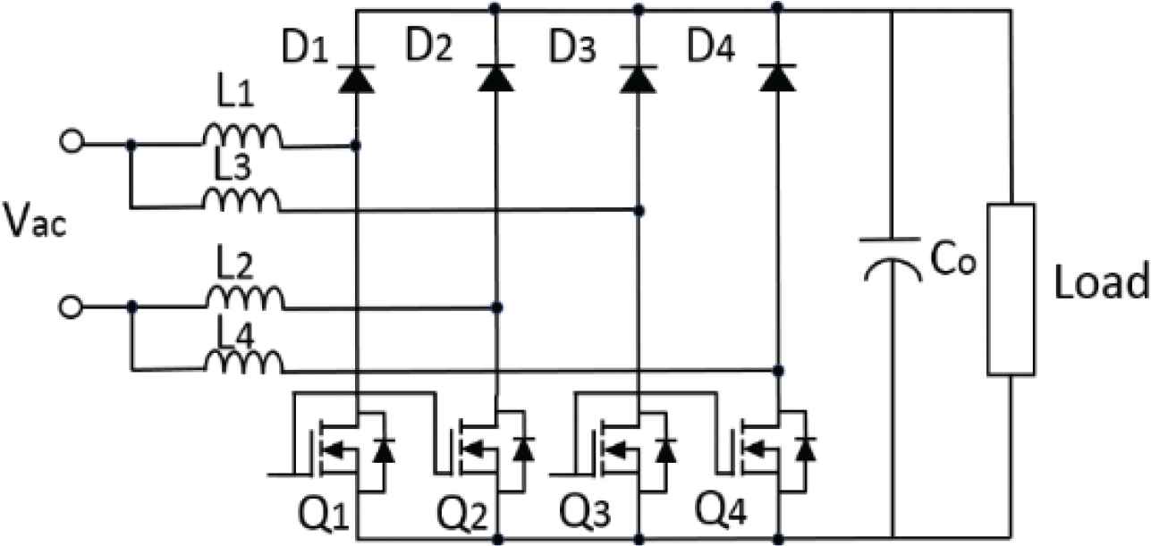
Bridgeless interleave PFC converter.
2. OPERATING ANALYSIS
The proposed current fed bridgeless interleave PFC boost converter with voltage doubler characteristic is shown in Figure 2. The operating and steady-state circuit analysis of the novel PFC converter was implemented with the AC line input during the positive half cycle. In the symmetrical control operating period of positive half cycle, the test condition of duty cycle (0 < D < 0.5) is analyzed, and the test condition of duty cycle (0.5 < D < 1) will be neglected due to the similar behavior. We supposed that the semiconductor components are ideal and then the circuit operating of the proposed PFC in one switching cycle will be discussed.
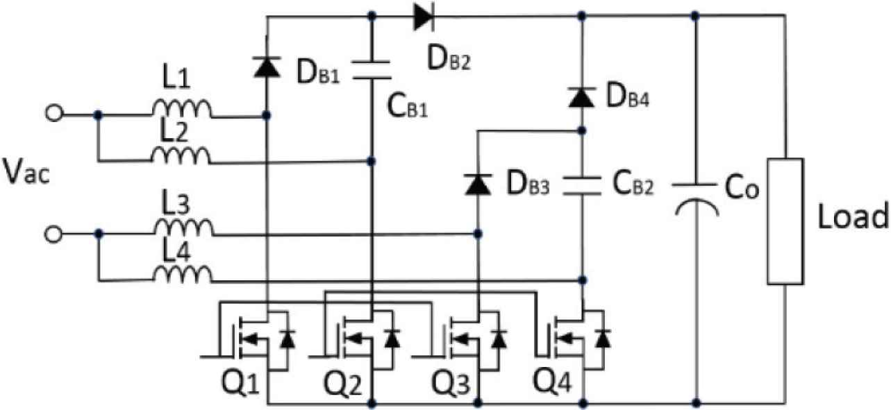
The proposed current fed bridgeless interleave PFC boost converter with voltage doubler characteristic.
A. The range of duty cycle (0 < D < 0.5)
In order to easy to obtain the stable analysis of the proposed PFC converter, the voltage and current operational waveforms are shown in Figure 3.
Period 1[t0 − t1]: The ripple current of L1, L3
The ripple current of L2, L4
Period 2[t1 − t2]: The ripple current of Q1, Q3 and current of L1, L3 increase linearly.
The ripple current of L2, L4
Combine (3) and (4), the total input ripple current ΔIin is the ripple current of addition of L1, L3 and L2, L4
Period 3[t2 − t3]: The ripple current of L1, L3
The ripple current of L2, L4
Period 4[t3 − t4]:
The ripple current of Q2, Q4 and current of L2, L4 increase linearly as well.
When Q1, Q3 turn off, current of Q1 is zero and ripple current of Q3 is the same as that of L3 current of L1 turns to increase linearly
Advance to combine (8) and (9), the total input ripple current ΔIin is the current of addition of L2, L4 and L1 and L3
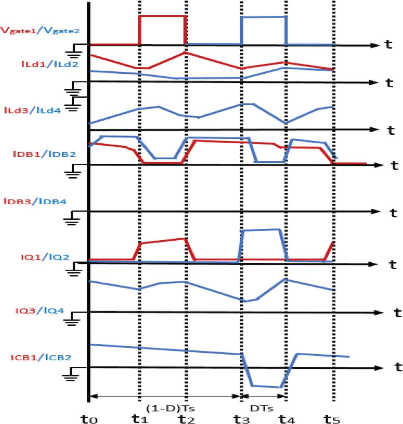
Operational waveforms of proposed converter during duty cycle 0 < D < 0.5.
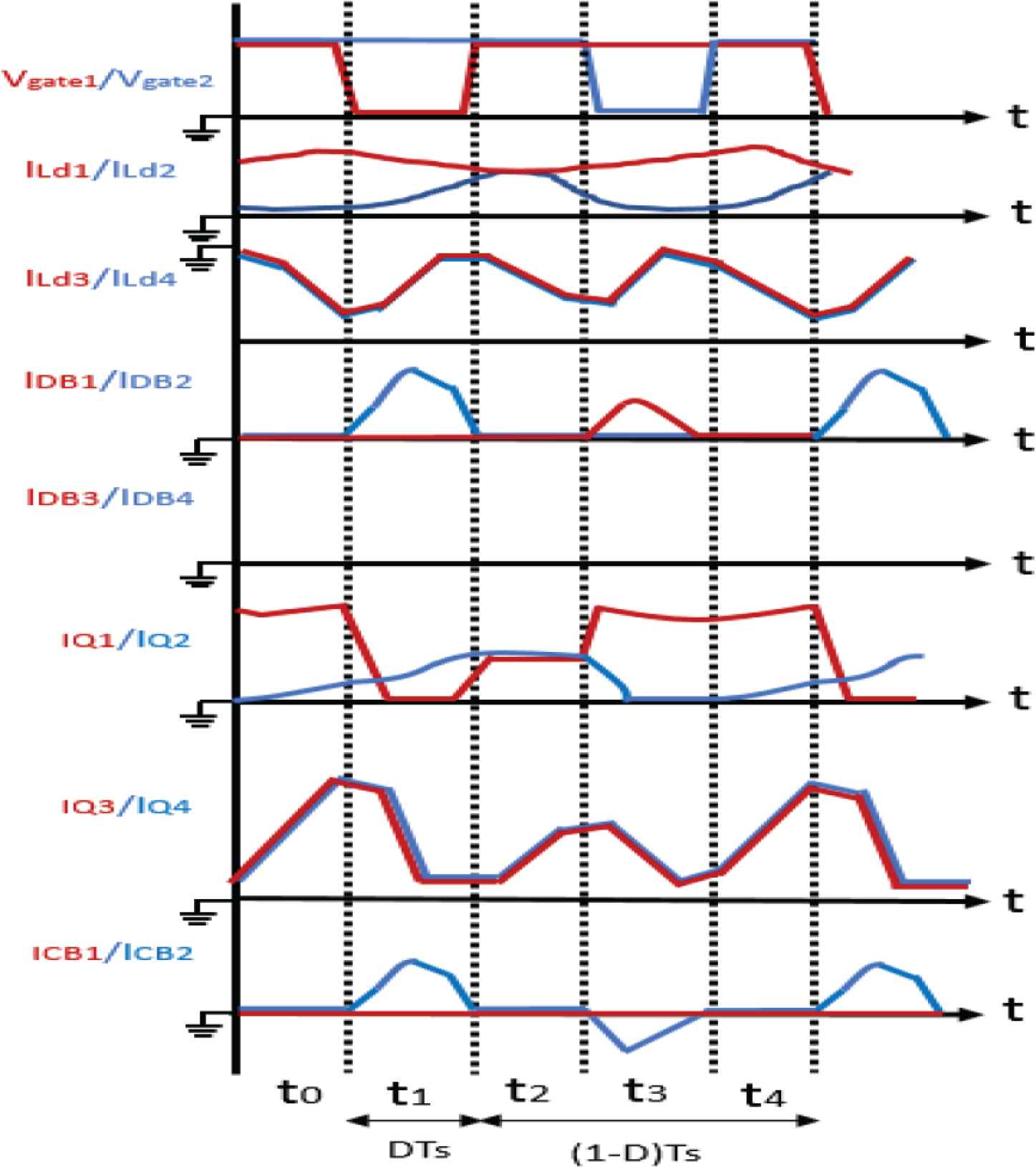
Operational waveform of proposed converter during duty cycle 0.5 < D < 1.
B. The range of duty cycle (0.5 < D < 1)
In this state, the voltage and current operational waveforms are shown in Figure 4.
Period 1[t0 − t1]: The ripple current of Q1, Q3 and current of L1, L3 increase linearly.
The ripple current of Q2, Q4 and current of L2, L4 also increase linearly, as (12) stated
Period 2[t1 − t2]: The ripple current of L1, L3 is
At the meantime, the ripple current of L2, L4
Combine (13) and (14), the total input ripple current ΔIin is the current of addition of L1, L3 and L2, L4
Period 3[t2 − t3]: current of L1, L3 increase linearly, as (16) stated
The ripple current of L2, L4 increase linearly as well.
Period 4[t3 − t4]: The ripple current of L1, L3 is
The ripple current of L2, L4
Combine (18) and (19), the total input ripple current ΔIin is the ripple current of addition of L2, L4 and L1, L3
3. SYSTEM VOLTAGE CONVERSION ANALYSIS
According to the circuit analysis of the proposed PFC converter, the equivalent equation will reveals when the current of L2, L4 increase
Based on Equation (21), we suppose L = L2 = L4 and
When current of L2, L4 decrease, the equivalent equation refer to (23) as
From Equation (23), we suppose L = L2 = L4 and
To analyze the current of L2 via the volt-second balance principle in Figure 4.
The voltage conversion ratio is obtained
According to the above voltage conversion equation, higher voltage gain ratio can be obtained while duty ratio D > 0.5 and the current of L2 decrease relatively according to Equation (24). Moreover, we can actually implement the similar derivation for the range of duty cycle (0 < D < 0.5). Eventually, the voltage conversion ratio is obtained in below
According to Equation (27), we can probably set up the lowest limit of duty ratio for avoiding the uncontrolled duty ratio in the proposed converter. Setting the duty ratio to 10%, and then the output voltage Vo is 11 times of VAC. As a result, the minimum duty ratio of the proposed converter will be 10% and the voltage gain is raised to 11. Figure 5 illustrates the voltage conversion gain ratio of the proposed converter.
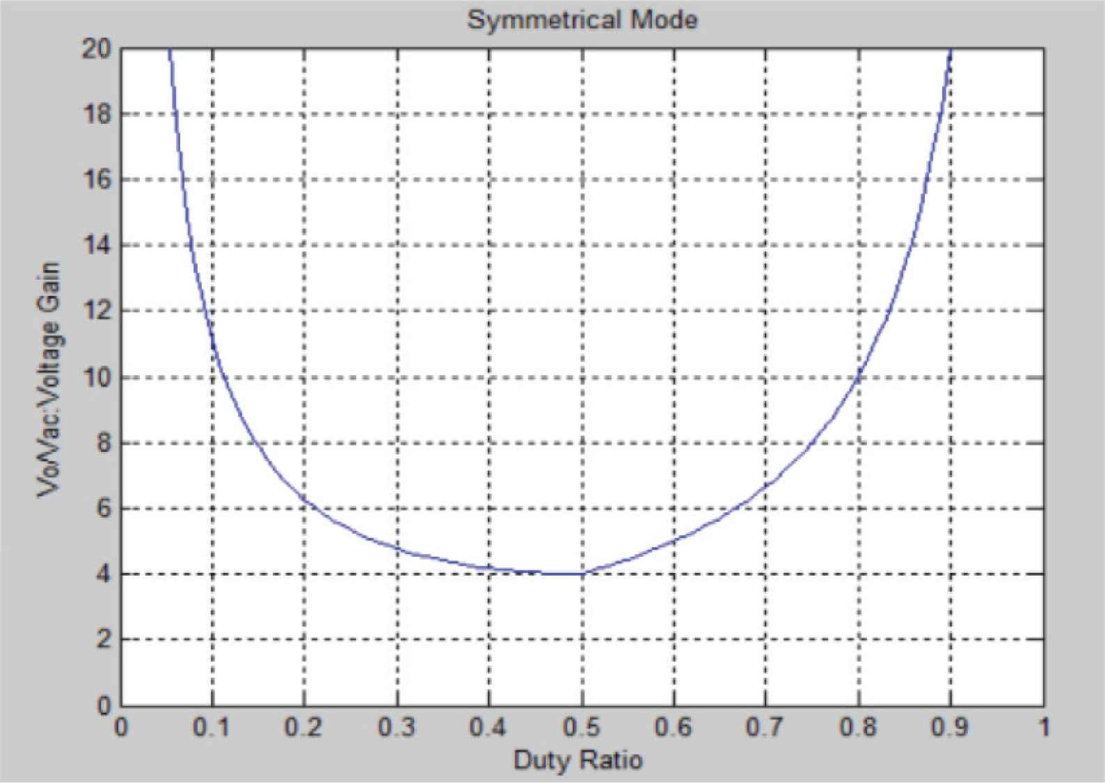
Voltage conversion gain ratio of the proposed converter.
4. SIMULATION RESULT
A set of 3.4 kW prototype was designed including design includes full range input 85–264 Vrms and 400 V/8.5 Å output electrical characteristic. Figure 6 was the efficiency comparison for AC input of 85 and 264 Vrms respectively. In this Figure, when the power lower than 1.5 kW at 85 Vrms input condition, the efficiency of the proposed converter higher than the conventional one. The reason is that the proposed converter operates in double voltage mode (voltage conversion ratio Vo/VAC = 2/(1 − D)) at duty ratio D > 0.5. The switches conduction loss of the proposed converter is about two-third of the conventional one. The switching loss of the switches and reverse recovery loss of the diodes are lower as well. This is because the voltage of switches and diodes are half of the output voltage. Furthermore, the efficiency of the proposed converter is higher than the conventional one when the converters operate in high line condition (264 Vrms).
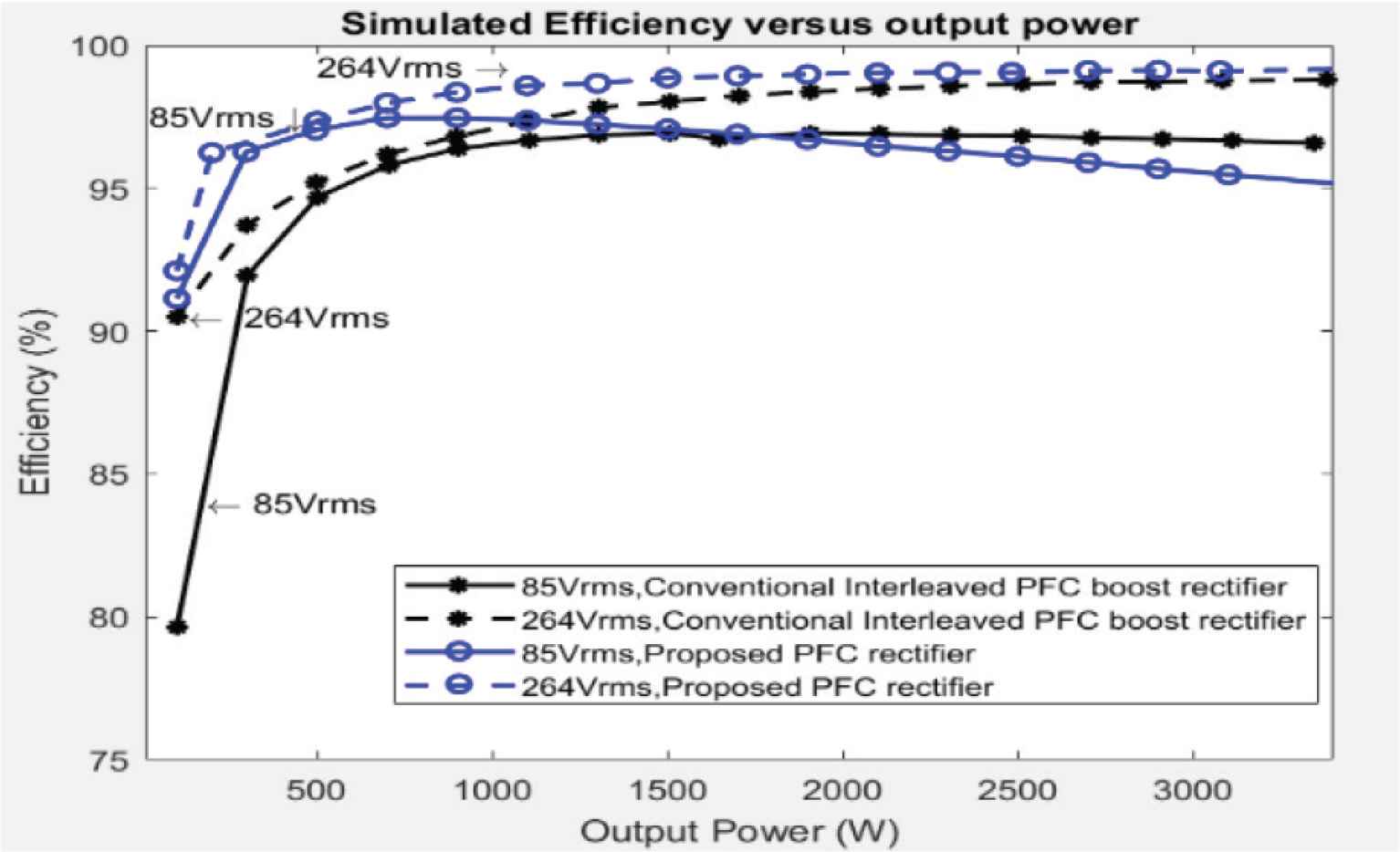
Simulation result of comparison of efficiency of the proposed converter and conventional interleave bridgeless PFC converter.
In this condition, the duty ratio is always higher than 0.5 and the voltage doubler characteristic is revealed. The simulation waveforms of output voltage Vo at Po = 3.4 kW and Vo = 400 V; input voltage Vin and input current Iin was stated in Figure 7. Based on the result that the efficiency of the proposed converter can reach 98% during 264 Vrms input voltage and out power of 0.5–3.4 kW condition, heat sinks and active cooling system can be reduced. Charging time and cost of power conversion can be reduced as well. Figures 8 and 9 simulate THDi and PF during input voltage range 85–264 Vrms. In Figure 8, it can be observed that the low line operated THD of proposed converter is lower than the conventional one while it is opposite when operated in high line. The PF of the proposed converter revealed in Figure 9 is lower than the conventional one.
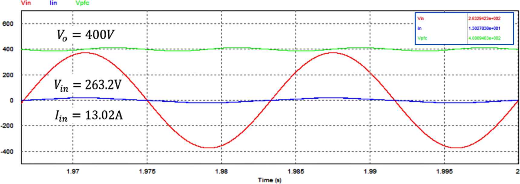
The simulation waveforms of output voltage Vo at Po = 3.4 kW and Vo = 400 V; input voltage Vin and input current Iin for the proposed converter.
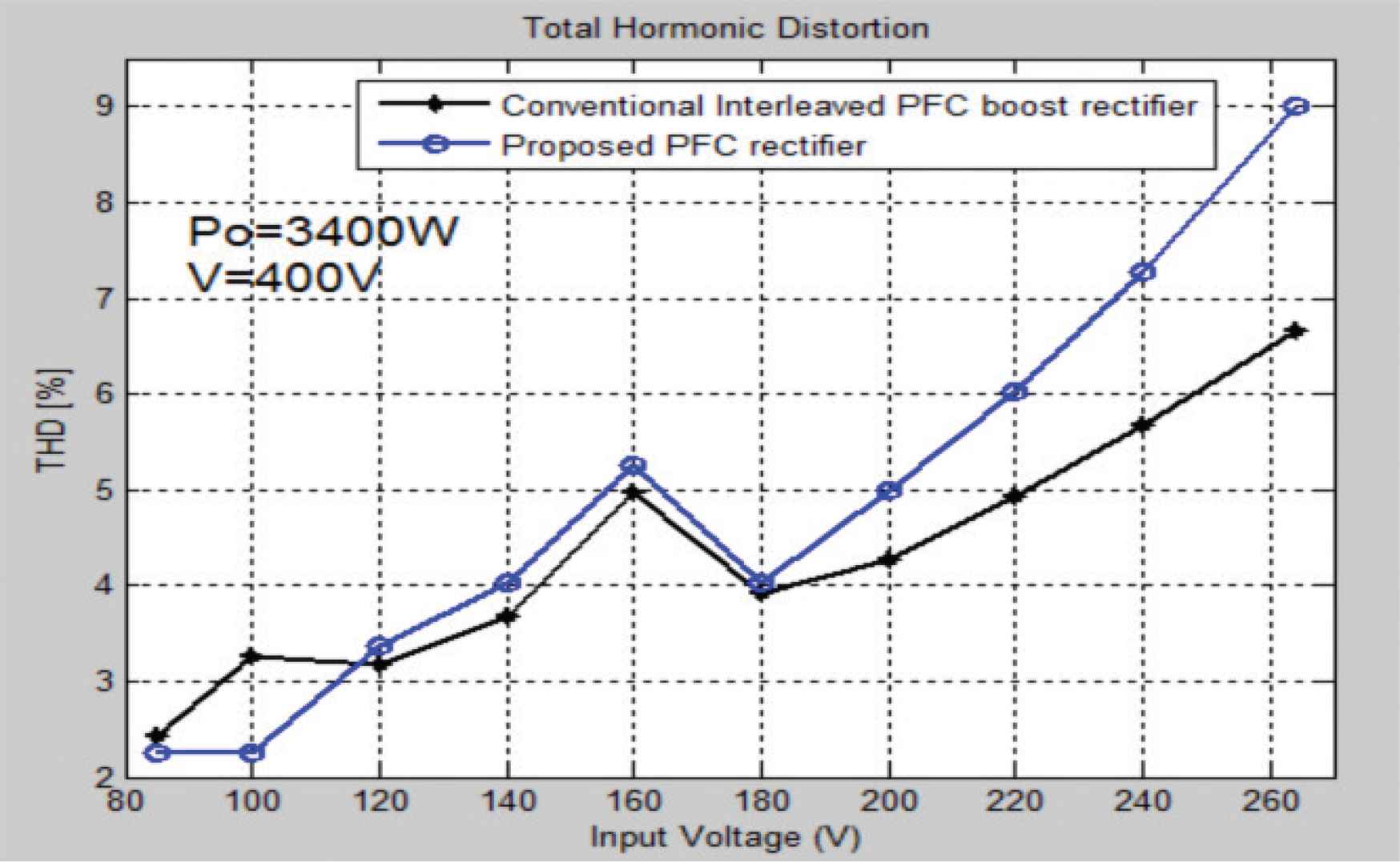
The comparison of THD simulation result of Po = 3.4 kW and Vo = 400 V for both converters.
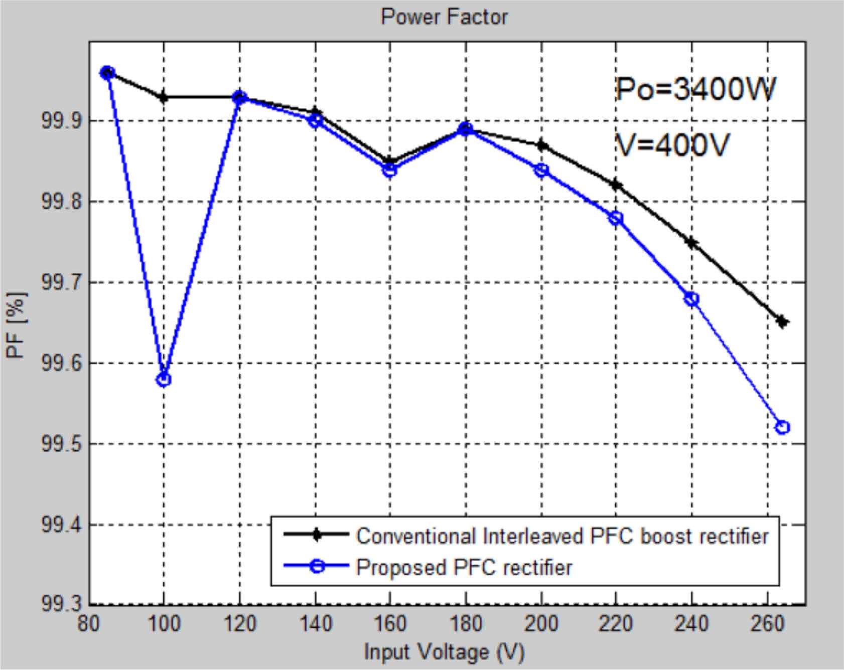
The comparison of PF simulation result of Po = 3.4 kW and Vo = 400 V for both converters.
5. CONCLUSION
In this paper, a current fed PFC boost converter with voltage doubler characteristic was proposed to apply for preliminary stage AC to DC converter of hybrid electric vehicle. The proposed PFC converter possesses high conversion efficiency when operates in low line condition. The proposed converter prototype was simulated and analyzed including efficiency, THD, and PF. Comparison was made for full-range input voltage, full load 3.4 kW and 400 V output test conditions. The efficiency reaches 97% when it was operated at 70 kHz switching frequency, 264 V input voltage, and 0.5–3.4 kW output power. The proposed converter possesses higher efficiency than conventional converter and suitable for applying as option of electric vehicle industry.
CONFLICTS OF INTEREST
The authors declare they have no conflicts of interest.
AUTHORS INTRODUCTION
Prof. Chih-Chiang Hua
 He (S’91–M’92) received the BS degree in Electrical Engineering from National Cheng Kung University, Tainan, Taiwan, in 1984, and the MS and PhD degrees in Electrical Engineering from the University of Missouri, Columbia, MO, USA, in 1990 and 1992, respectively. Since 1992, he has been with the National Yunlin University of Science and Technology, Douliou, Taiwan, where he is currently a Professor at the Department of Electrical Engineering. His research interests include power electronics converters, uninterruptible power supplies, and photovoltaic/wind energy systems. He is a Member of the IEEE Power Electronics and the IEEE Industrial Electronics Societies.
Prof. Ching-Chun Chuang
 He received the PhD degree in Electronics Engineering from National Taiwan University of Science and Technology, Taiwan, in 2013. Since 2017, he has been an Associate Professor at Faculty of College of Future, Yunlin University of Science and Technology, Taiwan. His research interests include power electronics, digital control and robot applications.
Dr. Hung-Chi Lee
 He received the MS and PhD degrees in Electronics Engineering from National Taiwan University of Science and Technology, Taiwan, in 2007 and 2013, respectively. He is currently a Postdoctoral Researcher of National Taiwan University of Science and Technology, Taiwan. His research interests include power electronics and EMC.
Prof. Chih-Wei Chuang
 He (1979) received the PhD degree in Electrical Engineering from National Yunlin University of Science and Technology, Taiwan, in 2017. Since 2017, he has been an Associate Professor at Faculty of College of Future, Yunlin University of Science and Technology, Taiwan. His research interests include the design and implementation of renewable energy sources and active power filters.
Mr. Chuan-Ming Niu
 He received Bachelor’s degree in Engineering (Energy Information Group) from Southern Taiwan University of Science and Technology in Taiwan in 2019. He currently study in a Master’s degree from the Graduate School of Engineering, National Yunlin University of Science and Technology, Taiwan. His research interests include Power Electronics and Power Systems.
REFERENCES
Cite this article
TY  - JOUR
AU  - Chih-Chiang Hua
AU  - Ching-Chun Chuang
AU  - Hung-Chi Lee
AU  - Chih-Wei Chuang
AU  - Chuan-Ming Niu
PY  - 2020
DA  - 2020/05/15
TI  - Research on a Bridgeless Interleaved PFC Boost Converter with Voltage Doubler Feature
JO  - Journal of Robotics, Networking and Artificial Life
SP  - 7
EP  - 11
VL  - 7
IS  - 1
SN  - 2352-6386
UR  - https://doi.org/10.2991/jrnal.k.200512.002
DO  - 10.2991/jrnal.k.200512.002
ID  - Hua2020
ER  -