
UWB, miniaturized and directive metamaterial loaded antenna for satellite applications
- DOI
- 10.2991/ijndc.2018.6.1.3How to use a DOI?
- Keywords
- Antenna; Metamaterial; Negative refractive index; RMPA; HFSS
- Abstract
Antenna parameter optimization using S-shaped metamaterial embedded in antenna substrate at high frequency (THz) is elucidated in this paper. Upon incorporation of proposed metamaterials’ array inside the antenna substrate, bandwidth of antenna increases by 770 GHz and directivity by about 11%. Results obtained are well in coherence between FEM based Ansoft HFSS simulation and Matlab programming based on CAD formulas using equivalent circuit analysis of patch antenna. A low frequency (scaled) prototype of the proposed structure is fabricated and nearly 15% deviation is obtained in comparison with the simulation results.
- Copyright
- Copyright © 2018, the Authors. Published by Atlantis Press.
- Open Access
- This is an open access article under the CC BY-NC license (http://creativecommons.org/licences/by-nc/4.0/).
1. Introduction
‘Metamaterials’ (MTMs) are engineered to modify the bulk permeability and/or permittivity of the medium [1]. They are realized by placing periodically, structures that alter the material parameters, with elements of size less than the wavelength of the incoming electromagnetic wave. This results in “meta” i.e. “altered” behavior or behavior unattainable by natural materials [2]. Particle shape has effect on the value of negative permittivity corresponding to Frohlich resonance. The geometry of negative permittivity particle has a strong effect on its surface plasmonic properties.
The software tool HFSS is used because it is a high performance full wave electromagnetic (EM) field simulator for arbitrary 3D volumetric passive device modeling [3].
This paper abridges the design of RMPA with resonant frequency 43 THz and operating frequency range of 38 THz to 48 THz having RT Duroid (εr=2.33) as substrate material in Section 2 by using Finite Element Method based Ansoft HFSS software and parametric study using equivalent circuit analysis in Matlab. Section 3 describes DNG MTM (S shaped) having negative refraction in the same frequency range. Section 4 mathematically demonstrates the resonant frequency of S- shaped MTM using internal inductances and capacitances from circuit diagram. Section 5 elucidates upon its application in antenna parameter optimization by embedding it in substrate. Section 6 concludes the trade-offs in achieving bandwidth enhancement in RMPA with DNG material in substrate.
2. Rectangular Microstrip Patch Antenna Design
2.1. Design
RMPA i.e. Rectangular Microstrip Patch Antenna, as the name implies consists of a rectangular patch over a microstrip substrate. Its major disadvantage is relatively low-impedance bandwidth which limits the field of application of these antennas. Metamaterials are embedded in the middle of its substrate to increase the bandwidth of antenna without altering its parameters and without much effecting the antenna’s radiation properties. Henceforth, metamaterial based antennas are introduced.
Transmission Line model represents RMPA as two slots of width, w, and height, h, separated by transmission line of length l. Thus, it is a non-homogeneous structure made up pf two dielectrics i.e. substrate and air. This shows that substrate and air will have different phase velocity and the dominant mode of propagation will be quasi-TEM. Therefore, effective permittivity, εeff, comes into consideration. There is fringing effect at the edges of patch, due to which the patch appears to be longer. So, Leff, i.e. effective length is defined which is obtained by adding 2Δl (additional length Δl due to fringing on each end) to the length obtained by using mathematical design equations [4]. Ground plane has length lg, and width wg. The tangential components of electric field are in phase. Therefore, maximum radiated field is normal to the surface of the structure. However, normal components of the electric field at the two edges along the width out of phase. Hence, no radiation in broadside direction. As per transmission line model ground plane should be infinite in extent. Practically, ground plane is finite with size greater than the patch dimensions by approximately six times the substrate thickness.
Microstrip feed using quarter wave transformer has been used for feeding the antenna as calculated from equation 1. The input impedance is taken at the base of microstrip feedline and is referred to 50Ω. i.e. Zo.
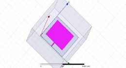
The operating frequency range of the designed antenna is 38THz to 48 THz with centre frequency 43THz. The substrate is RT Duroid 5870 (εr =2.33) as shown in Figure 1.
Rectangular microstrip patch antenna
Using design parameters, the patch antenna is designed in Ansoft HFSS with air box enclosing it with almost 10 times the size of antenna and having radiation boundary as shown in Figure 2.
RMPA design in HFSS
Constructional details are shown in Table 1.
| Frequency range | 38–48THz |
|---|---|
| Center frequency | 43THz |
| εr | 2.33 |
| εeff | 2.04 |
| h | 0.5 µm |
| w | 2.7 µm |
| Leff | 2.44 µm |
| ΔL | 0.25 µm |
| L | 1.94 µm |
| Lg | 4.34 µm |
| Wg | 5.7 µm |
| Lqw | 1.25 µm |
| Wqw | 0.5 µm |
| Lzo | 2.4 µm |
| Wzo | 1.6 µm |
Design parameters of RMPA
2.2. Simulation results using Ansoft HFSS
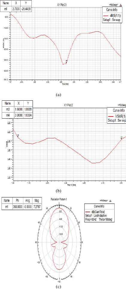
RMPA for ‘S’ shaped MTM has been simulated in HFSS. Figure 3 shows the simulation results where S11 is return loss or reflection coefficient.
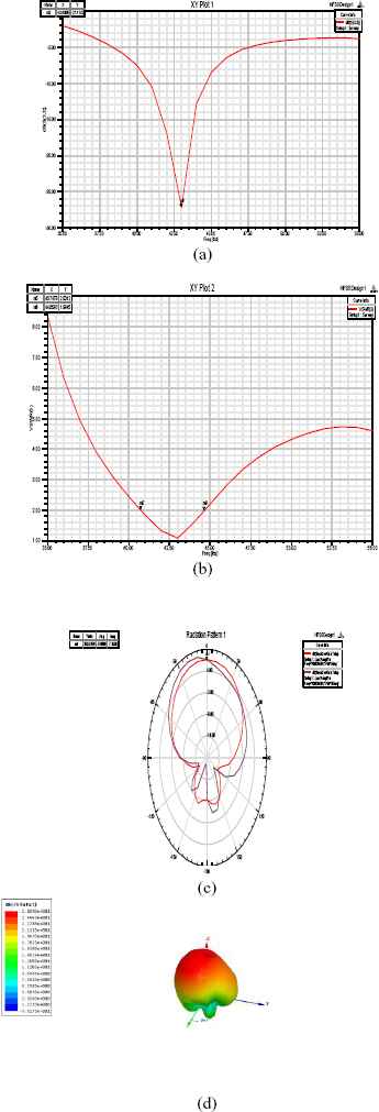
RMPA for ‘S’ shaped MTM: a) Return loss b)VSWR c) radiation pattern in E and H plane of RMPA d) 3D radiation plot
Simulation results have been shown in Table 2.
| Parameters | RMPA |
|---|---|
| S11 (dB) | −27.11 |
| VSWR | 1.09 |
| Bandwidth (THz) | 3.92 |
| Realized Total Gain in dB | 7.16 |
| Peak directivity(dB) | 6.52 |
| Front to back lobe ratio | 14.38 |
Simulation results of RMPA at 42THz
It can be seen that S11 is crossing 10 dB line and VSWR is less than 2. Bandwidth is 3.92 THz, which is range of frequencies with VSWR < 2.
2.3. Simulation results using Matlab
Microstrip antennas (often called patch antennas) are widely used in the microwave frequency region because of their simplicity and compatibility with printed-circuit technology, making them easy to manufacture either as stand-alone elements or as elements of arrays [5]. The parametric study using the CAD formulas are fairly accurate for thin substrates and illustrate the basic principles. For thin substrates the CAD formulas may even be accurate enough for final design purposes. For thicker substrates these formulas can still be used for initial design work, with full-wave simulation tools used to complete the final design. Using CAD formulas and programming in Matlab by parametric study, results have been shown in Figure 4.
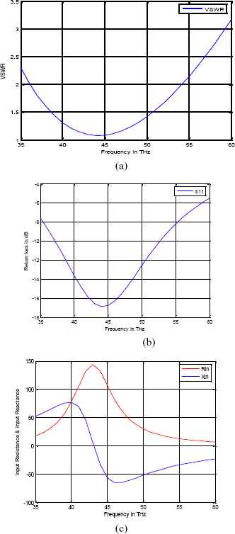
RMPA for ‘S’ shaped MTM: a) VSWR b) Return loss c) Input impedance vs frequency
It has been seen from Figure 4 that using CAD formulas for microstrip patch antenna in Matlab, we can initially plot the curve between input impedance and frequency. Thereby, we can obtain S11 and VSWR by applying the formulas, Reflection coefficient is ratio of (Zin−Zo)/(Zin+Zo) and VSWR is ratio of (1+abs(reflection coefficient))/(1−abs(reflection coefficient)).
From the curve of VSWR, the percentage bandwidth can be calculated by the percentage difference of lower and upper frequency bounds with the center frequency. Peak directivity can also be found using CAD formulas. The results obtained by coding in Matlab have been shown in Table 3.
| Parameters | Using Matlab | Using HFSS |
|---|---|---|
| S11 (dB) | −16.54 | −27.11 |
| VSWR | 1.096 | 1.09 |
| %Bandwidth | 11.09 | 9.09 |
| Peak directivity(dB) | 8.08 | 6.52 |
Simulation results of RMPA using Matlab
Thus, the results obtained from two different methods of analysis i.e. CAD formulas in Matlab and Finite Element Method in HFSS are well in coherence with each other. This shows that the parametric study using equivalent circuit analysis from which CAD formulas have been derived give nearly parallel results with Finite Element Method.
3. Proposed S-shaped metamaterial
In 1968, Russian scientist Veselago [6] postulated a negative material and theoretically proved the phenomenon that a uniform plane-wave followed the left-hand rule in a medium with negative permittivity (ε) and negative permeability (μ). The first work in this direction was by Pendry. He created a medium consisting of thin wires arranged in a periodic array [7]. These wires acted as a plasma medium, whereby ε varies with frequency, Pendry next achieved a negative μ with a periodic array of metallic loops called Split Ring Resonators [8]. In a medium composed of these rings the permeability, μ, varied with frequency, and could become negative. In 1999, Smith combined the rod and ring materials to finally produce a material with simultaneously negative ε and μ, a left-handed material [9]. The wire strips affect the ε and the split-ring resonators (SRRs) alter the μ of the medium thus giving a frequency dependent negative material with both the parameters negative. The wire medium and the SRRs have certain frequency dependence. The rod gives negative permittivity, ε, and ring material creates a negative permeability, μ, this combined rod and ring material gives negative index of refraction.
S shaped metamaterial has been proposed having bianisotropy. It behaves as DNG i.e. Double Negative Group.Such materials have negative permittivity and negative permeability in the same frequency region. Thus having negative refraction in the same [10], [11].
The parameter retrieval i.e. parameter extraction using S parameters [12] has been followed using NRW approach to observe the negative refraction region of MTM. The constructional details along with the curve showing negative refraction are as under.
3.1. Constructional Details
It is constructionally very simple, consists of a S shaped conductor on top and bottom surface of a RT Duroid Substrate, such that it looks like Figure of eight from top view[13],[14].Thus two opposite S-shaped metallic strips divide the unit cell into three regions[15].Unit cell formed in HFSS is shown in Figure 5(a) with constructional details in Figure 5 (b) where σs is the resistance of the metallic strips in each loop and F is to be the fractional volume of the cell occupied by either the top or bottom loop of the ‘8’ pattern. The dimensions of a unit cell are in the ‘a’ in the x direction, ‘b’ in the y direction, and ‘l’ in the z direction. Thus, in the xy plane, S = ab, is the area of a periodic unit. From the structure, we assume F1 to be the fractional volume of the cell occupied by the top loop of the 8 pattern (Area I, Loop 1), F2 to be the fractional volume of the cell occupied by the bottom loop of the 8 pattern (Area II, Loop 2), and F3 to be the fractional volume of the cell not enclosed by the rings (Area III). Therefore, F1 + F2 + F3 = 1.
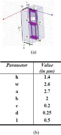
S shaped MTM a) unit cell designed in HFSS b) constructional details with σs=0.5ῼ and F =0.3
3.2. Simulation Results
Ansoft HFSS has been used to simulate the unit cell designed in Figure 6(a). Upon simulation it was found that at center frequency 36THz S11 (reflection coefficient) is −37.5504dB, S21 (transmission coefficient) is −1.6905dB. The boundaries and lumped ports (1 and 2) have been assigned as per Figure 6(a),(b),(c).
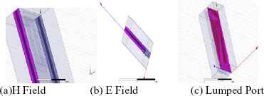
a) H field b) E field specifying boundary condition c) Lumped Port
Nicolson Ross Wier method has been used to calculate the material properties from transmission and reflection coefficients.
It can be observed as in Figure 7 (a), (b), (c), (d) that region of negative permeability extends from 37.5THz to around 54THz, the region of negative permittivity extends from 37.5 THz onwards, region of negative refraction can also be observed from 37.5THz to around 54THz, in the same region positive real impedance can also be noted.
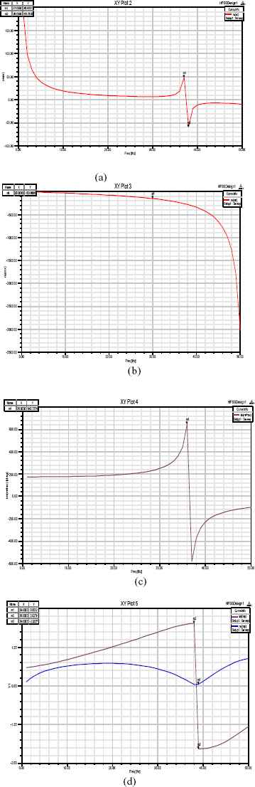
a) Resonance in permeability from 37.5THz to 54THz b) Plasma frequency of permittivity is 37.5THz c) Negative refraction from 37.5THz to 54THz d) Real part of impedance is positive from 37.5THz to 54THz
3.3. Mathematical Proof
S shaped MTM has magnetic properties because of internal inductances and capacitances. It can be simplified in terms of two magnetic loops as shown in Figure 8(a). Using transmission line theory we can draw its equivalent circuit as in Figure 8 (b).
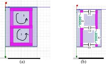
S-shaped MTM a) magnetic circuit loops b) equivalent circuit
As seen from Figure 8 (b), C2 is the capacitance between the center metallic strips, and C1and C3 are the capacitances of the top and bottom metallic strips respectively. Take the inductance per unit length in the z direction of each half ring to be L1 and L2.Assume C1=C3=C and L1=L2 and F1=F2=F3=0.3=F.
Let us solve the circuit by finding equivalent inductance and capacitances i.e. Leq and Ceq.
Leq is given by the area enclosed by each ring i.e.
From equation 2, L=4.07*10−6H
Using simple circuit theory, equivalent capacitance Ceq can be found out as
Thus, resonant frequency of S shaped MTM is given by using 2 and 3 as
Therefore, using equation 2 and 3 in 4 we get
Now the capacitance between two metallic strips can be calculated as
Putting values from Figure 5 (b) in equation 6 we get, C=1.983 *10−23F.
Substituting values of C and L in equation 4, we get magnetic resonance frequency, f0=31THz.
Also, the magnetic plasma frequency is given by
Upon substitution, fp=49THz.
Experimentally the value of magnetic resonance frequency has been found out to be 37.5THz and theoretically the value is 31THz. So, there is around 17% error in the simulation.
This rectangular microstrip patch antenna has been fabricated by scaling (by (1/10000) the above designs to low frequency. The substrate has also been changed to FR4. The fabricated antenna is shown in Figure. 9.
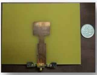
Fabricated Antennas: Microstrip Patch antenna
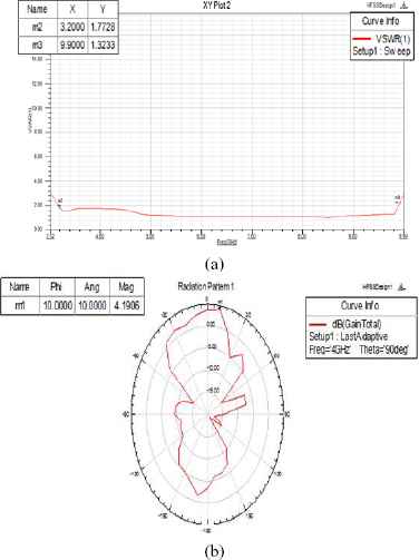
The above design is simulated in HFSS and results are shown in Figures 10.
Patch Antenna: a) Return Loss b ) VSWR c) Radiation Pattern
Using Keysight RF Fieldfox Network Analyzer as shown in Figure 11, the simulation and fabrication results are compared in Figure. 12.
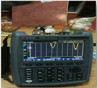
Keysight Fieldfox RF Network Analyzer
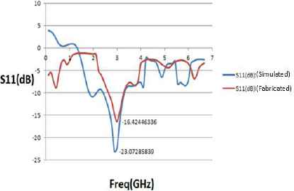
Return Loss of Patch Antenna
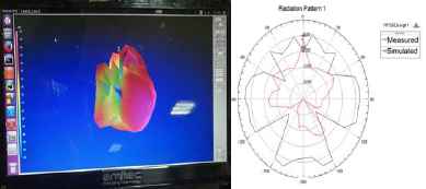
Using gain measurement set-up as shown in Figure 13, gain and radiation pattern have been obtained in Figure 14.
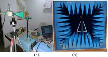
(a) Gain measurement set up for X band (b) Set up inside anechoic chamber
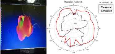
Radiation Pattern measurement of Patch Antenna
The above results have been tabulated in Table 4.
| Antenna Design | Gain (dB) | Directivity (dB) | Band-width (GHz) | Return loss (dB) |
|---|---|---|---|---|
| Patch Antenna (Simulated) | 1.9 | 5 | 1.3 | 23 |
| Patch antenna (Fabricated) | 1.7 | 4 | 1.5 | 16 |
Comparison of simulated and fabricated results for RMPA
Thus, “fabricated and simulated antennas” helps in achieving miniaturization and bandwidth enhancement which is in coherence with the proposed antenna configurations with nearly 10% error.
4. Antenna Parameter Optimization
4.1. Design
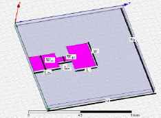
Antenna is characterized by different parameters e.g. gain, bandwidth, VSWR3dB beam width in E,H plane, return loss. These parameters have been obtained for RMPA as in table 2 using HFSS. Parameter optimization is done by embedding the proposed S shaped MTM 3X4 array as shown in Figure 15, having 0.55μm as Δx and 1.3μm as Δy inside the RMPA.
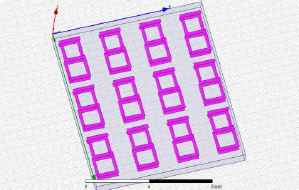
Embedding S-shaped MTM array inside RMPA substrate
Inserting proposed MTMs 3X4 array inside the RMPA substrate, such that the top patch of MTM is 0.125 μm down from the top of the substrate, will change the effective material parameters below the patch, thereby affecting the performance of the antenna.
4.2. Simulation
Simulation results for MTM Antenna with ‘S’ shaped MTM Array are shown in Figure 16.
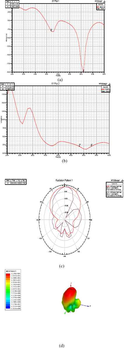
MTM Antenna: a) Return loss b) VSWR c) Radiation pattern in E and H plane of RMPA d) 3D radiation plot
Table 5 gives the obtained simulated values of parameters and comparison of S-shaped MTM RMPA with RMPA without MTM.
| ANTENNA/Parameters | RMPA | RMPA with S-shaped MTM |
|---|---|---|
| S11 (dB) | −27.11 | −19.99 |
| VSWR | 1.09 | 1.22 |
| Bandwidth (in THz) | 3.92 | 4.67 |
| Realized Total Gain in dB | 7.16 | 3.79 |
| Peak Directivity(dB) | 6.52 | 7.23 |
| Front to back lobe ratio(dB) | 14.38 | 19.91 |
Simulation and comparison results of S-shaped MTM embedded in RMPA substrate
Upon designing and analyzing proposed ‘S’ shaped MTM array inside RMPA substrate the results are tabulated as in Table 5. It can be seen that there is enhancement in bandwidth with S-shaped MTM by 770GHz. VSWR decreases up to 11%. The smaller the VSWR is, the better the antenna is matched to the transmission line and the more power is delivered to the antenna. Decrease in realized total gain as observed from the radiation pattern is 89%. Directivity improves by 43% and thereby reducing side lobes as can be observed from front-to-back lobe ratio of the antenna. The S-shaped metamaterial antenna has been fabricated by scaling (by (1/10000) the above designs to low frequency. The substrate has also been changed to FR4. The fabricated antenna is shown in Figure 17.
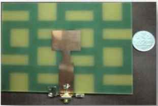
Fabricated Antennas of Swastika metamaterial Antenna
The above structure is designed and simulated in HFSS. The simulation results are shown in Figures 18.
S-shaped Metamaterial Patch Antenna: a) VSWR b) Radiation Pattern
The return loss and VSWR curves are studied using Keysight RF Fieldfox Network Analyzer as shown in Figure 19.
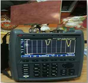
Keysight Fieldfox RF Network Analyzer
The simulation and fabrication results of return loss are compared in Figure 20.
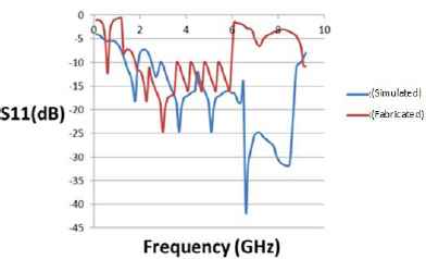
Return Loss of S-shaped metamaterial Patch Antenna
Using gain measurement set-up radiation pattern has been obtained in Figure 21.
Radiation Pattern measurement of Swastika metamaterial patch Antenna
The above results have been tabulated in Table 6.
| Antenna Design | Gain (dB) | Directivity (dB) | Bandwidth (GHz) | Return loss (dB) | Miniaturization (%) |
|---|---|---|---|---|---|
| S-shaped metamaterial RMPA, Simulated | 4.9 | 5 | 6.7 | 20 | 51 |
| S-shaped metamaterial RMPA, Fabricated | 4.8 | 4 | 4.2 | 25 | 84 |
Comparison of simulated and fabricated results for S-shaped metamaterial RMPA
Thus, “fabricated and simulated antennas” helps in achieving miniaturization and bandwidth enhancement which is in coherence with the proposed antenna configurations with 12 % error.
5. Trade-offs
In this paper, around 17% error has been computed between numerical simulations and theoretical calculations of S –shaped metamaterial. Using MTM array (3X4) inside RMPA, it can be seen that there is enhancement in bandwidth by 770 GHz, 11% reduction in VSWR and directivity increases by 11%. However, reduction in gain has also been observed. Also, no improvement in return loss can be seen. The increase in directivity accounts for reduction in front to back lobe ratio.
However, the coherence between equivalent circuit analysis using parametric study by applying CAD formulas in Matlab and Finite Element Method technique in HFSS has been observed.
Thus, we have been able to obtain more bandwidth, better and enhanced directivity at cost of realized total gain and VSWR for patch antenna with proposed MTM 3X4 array.
References
Cite this article
TY  - JOUR
AU  - Parul Dawar
AU  - N.S. Raghava
AU  - Asok De
PY  - 2018
DA  - 2018/01/02
TI  - UWB, miniaturized and directive metamaterial loaded antenna for satellite applications
JO  - International Journal of Networked and Distributed Computing
SP  - 24
EP  - 34
VL  - 6
IS  - 1
SN  - 2211-7946
UR  - https://doi.org/10.2991/ijndc.2018.6.1.3
DO  - 10.2991/ijndc.2018.6.1.3
ID  - Dawar2018
ER  -