
A Comprehensive Analysis and Hardware Implementation of Control Strategies for High Output Voltage DC-DC Boost Power Converter
- DOI
- 10.2991/ijcis.2017.10.1.10How to use a DOI?
- Keywords
- DC-DC boost converter; proportional-integral (P-I) controller; fuzzy controller; voltage-lift technology; HVDC power converter
- Abstract
Classical DC-DC converters used in high voltage direct current (HVDC) power transmission systems, lack in terms of efficiency, reduced transfer gain and increased cost with sensor (voltage/current) numbers. Besides, the internal self-parasitic behavior of the power components reduces the output voltage and efficiency of classical HV converters. This paper deals with extra high-voltage (EHV) dc-dc boost converter by the application of voltage-lift technique to overcome the aforementioned deficiencies. The control strategy is based on classical proportional-integral (P-I) and fuzzy logic closed-loop controller to get high and stable output voltage. Complete hardware prototype of EHV is implemented and experimental tasks are carried out with digital signal processor (DSP) TMS320F2812. The control algorithms P-I, fuzzy logic and the pulse-width modulation (PWM) signals for N-channel MOSFET device are performed by the DSP. The experimental results provided show good conformity with developed hypothetical predictions. Additionally, the presented study confirms that the fuzzy logic controller provides better performance than classical P-I controller under different perturbation conditions.
- Copyright
- © 2017, the Authors. Published by Atlantis Press.
- Open Access
- This is an open access article under the CC BY-NC license (http://creativecommons.org/licences/by-nc/4.0/).
1. Introduction
Traditional DC-DC boost converters widely utilized for high voltage direct current (HVDC) power transmission systems, transportation, electric vehicles (EVs) and hybrid electric vehicles (HEVs) applications [1–4]. But, the issues are persisting by the experimental study [3]. The EVs that are supplied by 42V batteries or storage devices require around 300V during start-up. Hence, the transient is increased for the DC-DC converter. Numerous topologies are proposed to meet the HV requirements, but almost all of them suffer deficiencies [1], [4–6]. A transformer-less DC-DC boost resonant converter topology with four switches in full-wave structure was investigated [7]. However, the switching frequency is limited up to 10 kHz in order to decrease the switching losses, but efficiency is limited [7]. Further, the converter topology that operates in cascaded structure of six MOSFETs was proposed to over HV requirements. But, which require a complex control algorithm to yield high voltage output [8]. Alternatively, the transformer based topologies to obtain HV gain with increased number of switches also was developed [9–10]. In this case, the transformer causes bulky structure and increased high-cost of the overall topology. Furthermore, the literature survey on HV DC-DC converters concludes that above topologies are drastically suffered by the reduction in gain and reduced output voltage. Approach by increased switch numbers make the control strategy much more complex that further causes lesser efficiency and increased costs [11–15].
To overcome these stated deficiencies, DC-DC converter with integrated voltage-lift techniques is recommended. The voltage-lift technique provides a staircase increment on output voltage by geometrical progressions [16–18]. Extra HV (EHV) DC-DC boost power converter which is obtained from the modified version of the classical buck. Power circuit is constituted with voltage-lift technique by including some additional passive (inductor/capacitor) components. Owing to its simple control algorithm and higher gain on output voltage [16–18]. The performance of the proposed EHV power converter adds the advantages as below [11–12], [18]:
- ▪
Increased output voltage-gain (k) ratio
- ▪
Simpler in control algorithm with wide range of operation
- ▪
Reduced ripple level at the output voltage and current
- ▪
Increased power density with efficiency
- ▪
Closed-loop controller requires only one sensor (voltage feedback) for investigated controlling aspects P-I and fuzzy logic
The hardware prototype of EHV DC-DC boost converter is implemented with a digital signal processor (DSP) TMS320F2812 platform. The main contribution of this study focused on simple development of the control strategy based on P-I and fuzzy logic controllers for its comparative performances under different line/load regulation conditions. The TMS320F2812 processor performs the closed-loop control algorithm of P-I and fuzzy logic, and PWM generation for N-channel MOSFET. The experimental results presented closely match with the analytical predictions.
This research manuscript is articulated here in below. Section 2 describes the circuit configuration of EHV boost power converter. Analytical developments during operational mode are elaborated in section 3. The characteristic of the converter configuration along with power loss calculation are given by section 4. Further, theoretical background and practical implementation are discussed in same section 4. Proposed control scheme based on P-I and Fuzzy Logic algorithm are illustrated in detail by section 5. Hardware prototype implementation using DSP processor and complete set of experimental results are presented in the section 6. Real time results are presented with different perturbation conditions along with theoretical background in the same section. Finally, the conclusions of this article are given by section 7.
2. EHV Boost Power Circuit Configuration
Fig. 1(a) shows the extra high voltage (EHV) DC-DC boost converter circuit. The load voltage (VO), load current (iO), the supply voltage (V1), supply current of the power circuit (i1) are depicted in the same Fig. 1(a). It consists of an N-channel MOSFET as static switch S, and diodes (D, D1,…, D13). The voltage-lift circuit is obtained by inclusion of additional capacitors (C, C0, C1, …, C4) and inductors (L, L0,…, L3) to the existing circuit. The voltage-lift gain is actually obtained by the capacitors (C2, C3, C4), where the capacitor voltage VC is built-up by four times (transfer gain ratio) of the battery input voltage V1 (VCO=VC1). In continuous conduction mode, it is assumed that all components are ideal, capacitors are large enough.
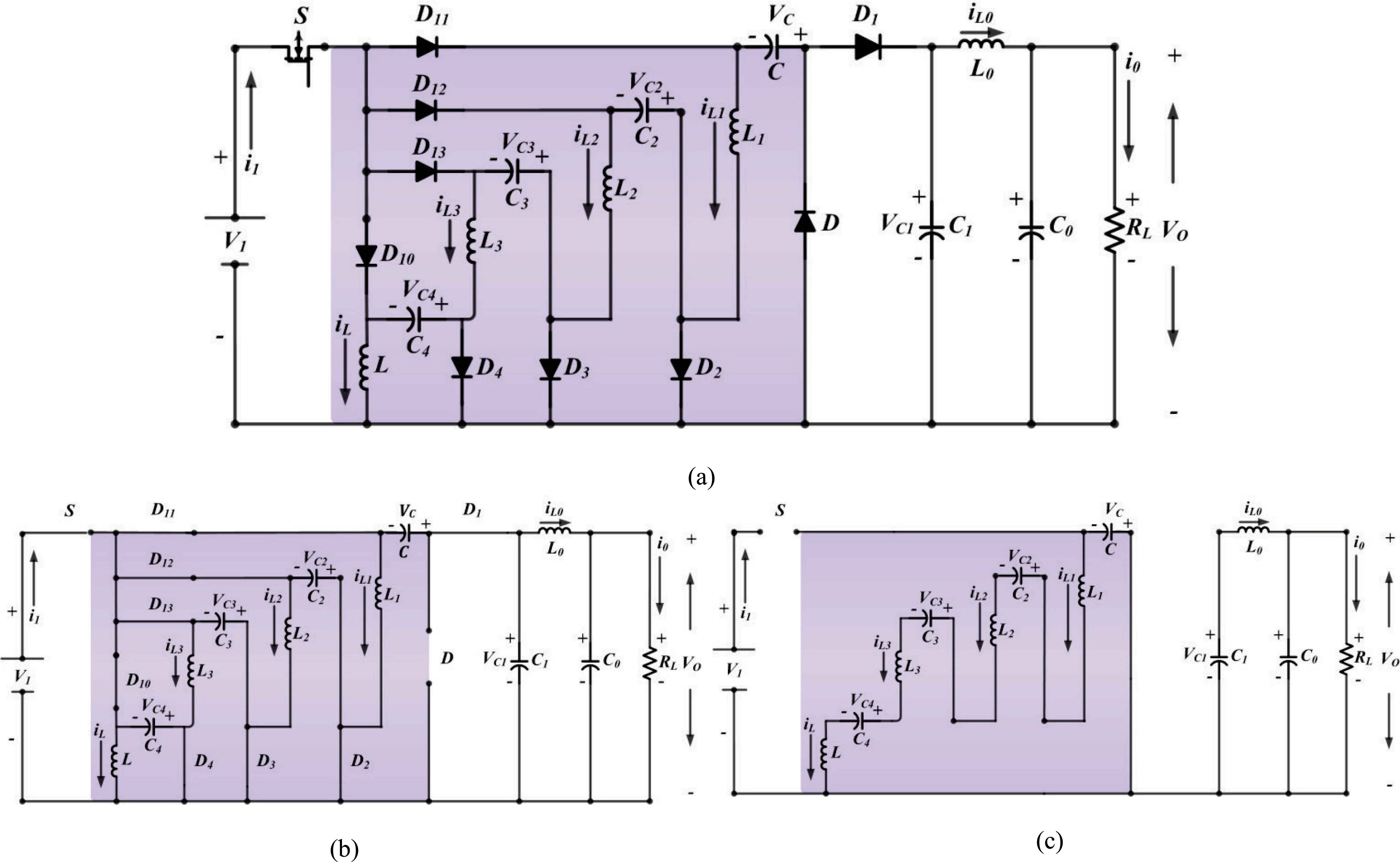
(a) Topology of extra high voltage (EHV) dc-dc boost power converter circuit; (b) Equivalent power converter circuit when switch turned ON; (c) Equivalent power converter circuit when switch turned OFF.
3. Analytical Prediction of Operating Modes
The first interval when the switch S is turned ON, corresponding equivalent circuit is shown in Fig. 1(b) with voltages and currents direction. The instantaneous input current (i1-source current) gets equal to sum of all capacitor and inductor currents, except iCO and iC1. The load current (iO-load) flows depending to the sum of the battery supply voltage V1 and the capacitor voltage VC.
Now, the capacitors C2, C3, and C4 are charged by the input voltage and all inductor currents which lead to first prediction of investigation are increased at this interval.
The corresponding equivalent circuit when switch S is turned OFF is shown in Fig. 1(c) along with voltages and currents direction. The instantaneous input current (i1-source current) equals to zero at this interval. The voltage-lift part that is located on the left-hand side of capacitor C (L1, L2, L3 and L), and inductor store the energy, while C2, C3 and C4 capacitor discharge the stored energy. Corresponding directions that are leading to charge the capacitor C are shown in the Fig. 1(c). The current iL0 flows through the load over the inductor and decreases the current with all the inductors which leads to second prediction of investigation. In steady–state, the average inductor voltage is zero, leading to:
The circuit voltages will be the same when switch S is turned ON:
It should be noted that the inductor current IL is increased when the switch S is turned ON and is decreased during switch S is turned OFF. The voltage components V1 as well –VL-OFF, which predicts that the voltages across the inductor L are expressed as follows:
The voltages across inductors (L1, L2, L3) are determined as the following:
Fig. 1(c) provides the analytical prediction of the capacitor voltage VC and output voltage VO as:
Again from Eq. 3,
Finally, the average voltages and currents are predicted and summarized as:
4. Characteristics and Power Loss Analysis
Table 1 summarizes the comparison between the EHV DC-DC boost converter and classical converter with respect to voltage-lift transfer
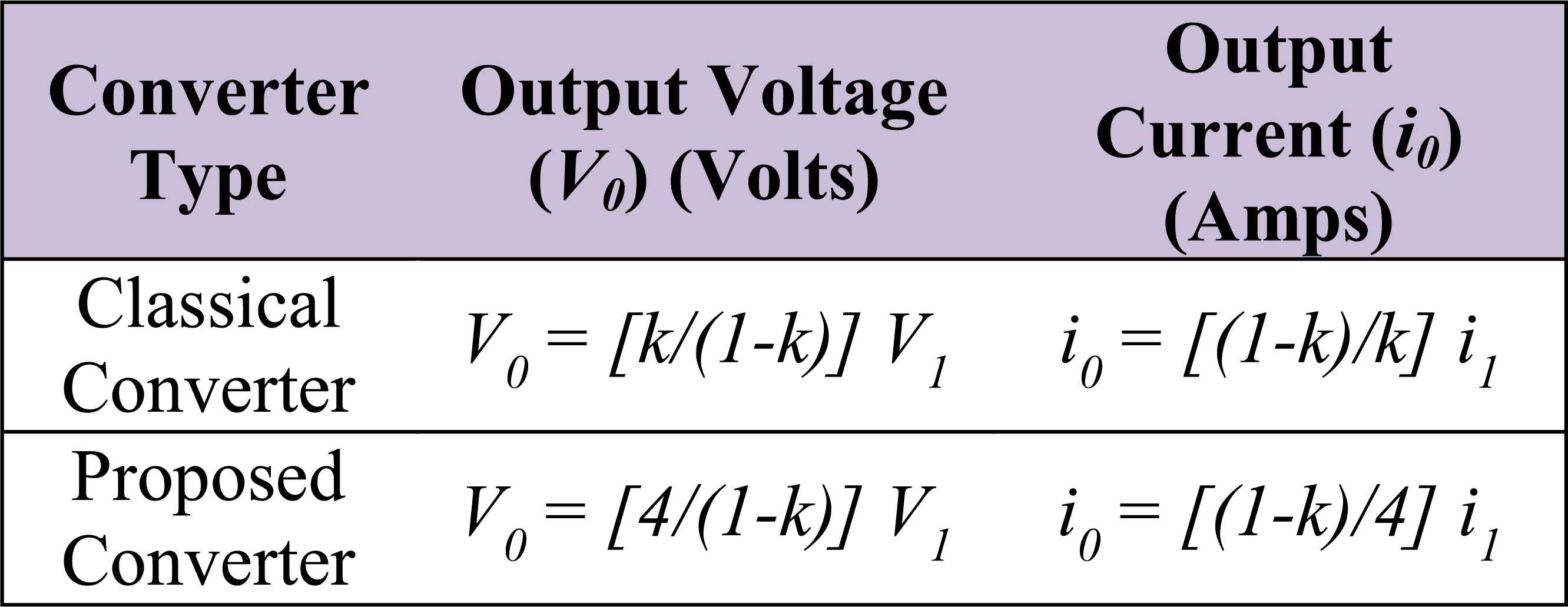
Comparative performances emphasis the proposed with classical dc-dc boost power converter.
Accordingly, Fig. 2 proves the effectiveness of proposed power conversion. As seen, the proposed DC-DC converter (red bar) output voltage varies from 44.44V to 400V, while for classical one (blue bar) varies from 1.11V to 90V when subjected to output transfer gain (duty ratio) k = 0.1 to 0.9 variation.
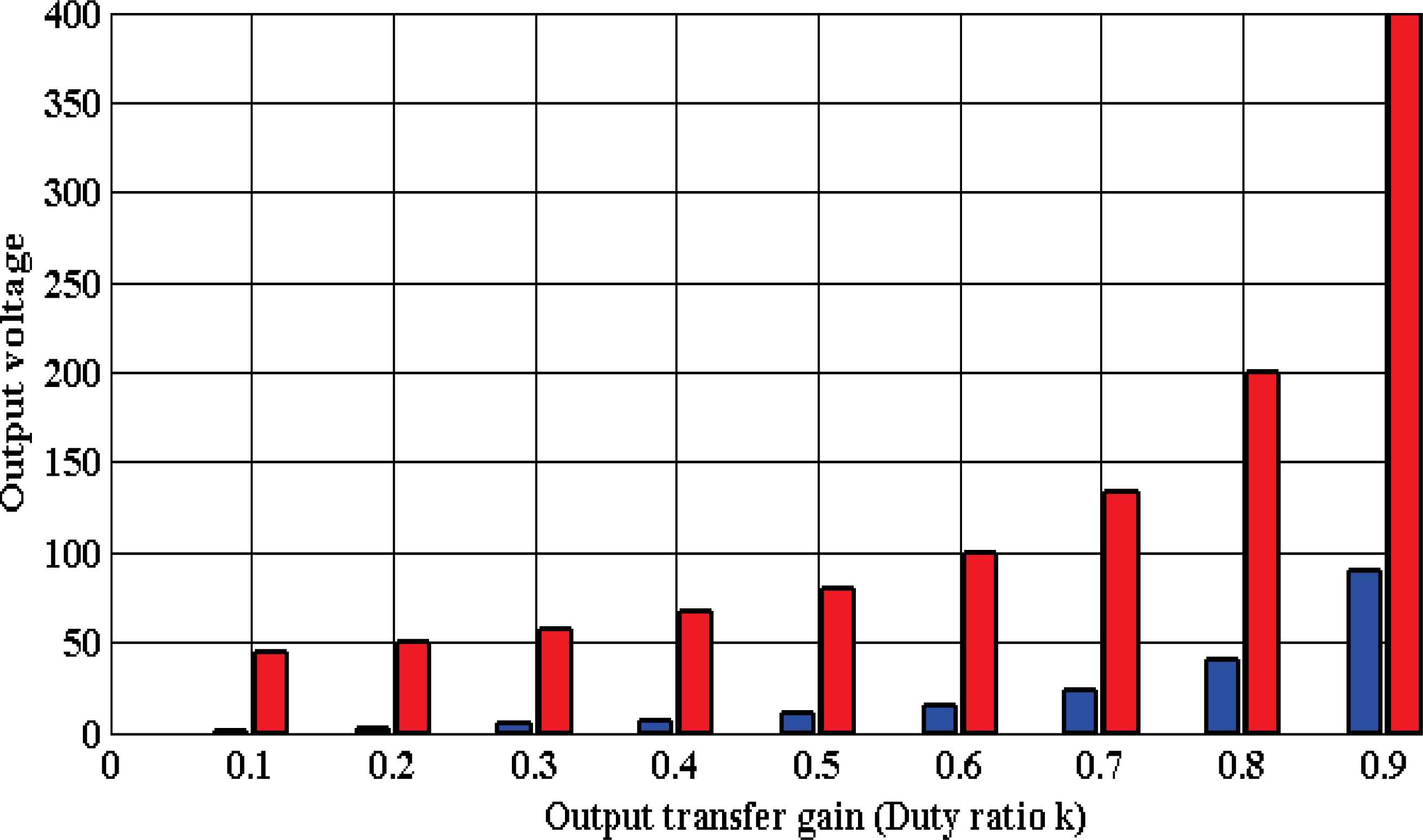
Comparative performances emphasis the variation of duty ratio k versus output voltage VO for the proposed power conversion (red bar) with classical power conversion (blue bar) unit (steady-state rated condition).
A complete set of performance outputs obtained from open-loop experimental tests by considering the parameters taken from Table 2 are summarized in Table 3. All operating conditions (duty cycle variation k= 0.1~0.9) the converter performed with efficiency of 99% in experimental test with reduced ripple content of 0.43% at the outputs is observed. Thus, the test parameters output voltage (VO), output current (iO) and efficiency (η) from the Table 2 confirms that obtained results are very closely matched with the theoretical background. To be noted, that the converter produced high efficiency due to the inclusion of additional passive (L, C) components actually reduced several parasitic effects (L, R, C, and MOSFET switching, conduction etc.) [21], which is proved by Eq.12. Further literatures, the inductance parasitic effects are neglected in DC-DC converters investigations. To attain high efficiency the RC time constant of converter is always compared to the switching frequency. Hence by considering the small parasitic inductance, the results could differ and the current is expressed as [19]:
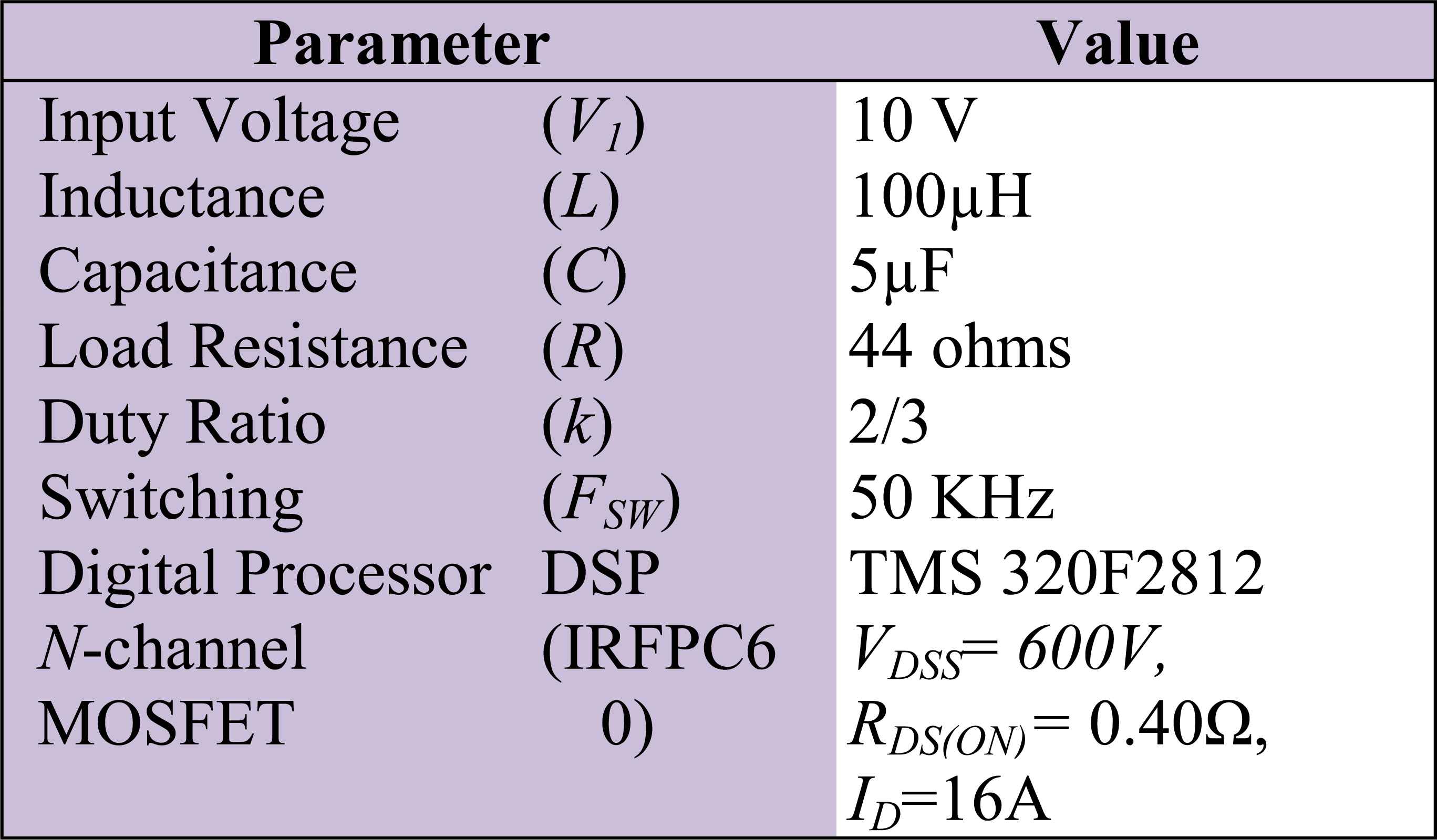
Simulation parameters taken for investigation.
Where iO, iint, and VO, are the load current, initial current, and initial voltage difference between the source voltage and capacitor, respectively. The conduction loss of the circuit is directly proportional to the square of the rms value. Hence the conduction loss of the MOSFET is calculated as:
Where, ION is the drain current, RDS,ON is the drain-source resistance of the MOSFET, in ON state. Therefore, by multiplying Eq. 24 by the duty ratio (k) leads to average value of the conduction loss. The switching losses of the MOSFET are calculated by the non-zero product of drain current (ID) and drain to source voltage (VDSS). If the MOSFET is assumed as ideal switch, the rise and fall time of the current and voltage, switching loss is zero. Then, the switching losses are determined by:
Where, VOFF is the drain source voltage, TSW,ON, TSW,OFF is the time to turn ON and turn OFF state, and FSW is the switching frequency of the MOSFET. From Table 2 and considering Eq. 24 and Eq.25, with duty ratio k=2/3 (i.e.TSW,ON = 2/3 * 1/50KHz, TSW,OFF = 1/3 * 1/50KHz) used for calculating the losses.
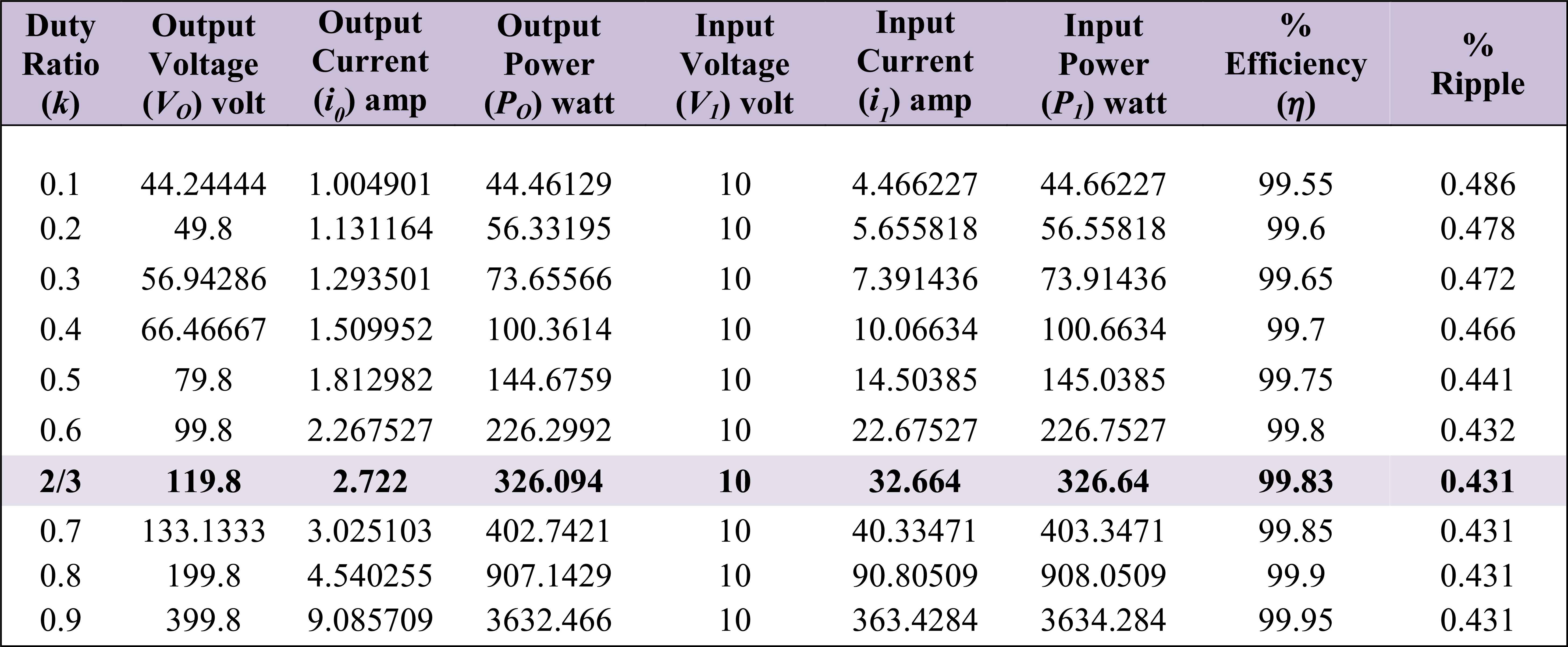
Investigated output performance indices of hardware prototype testing.
Fig. 3 and Fig. 4 illustrate the variation of conduction loss and switching loss, respectively, when parasitic L changes. It could be observed that the conduction losses are reduced dramatically at 100μH and correspondingly the switching loss is minimal at resonant point 100μH with inductance profile variation. Therefore this concludes that the increasing parasitic effects of power converters can be overcome by inclusion of additional passive components (L and C i.e. voltage lift technique) within the power circuit without any additional external compensation network/circuitry [11–17], [19].
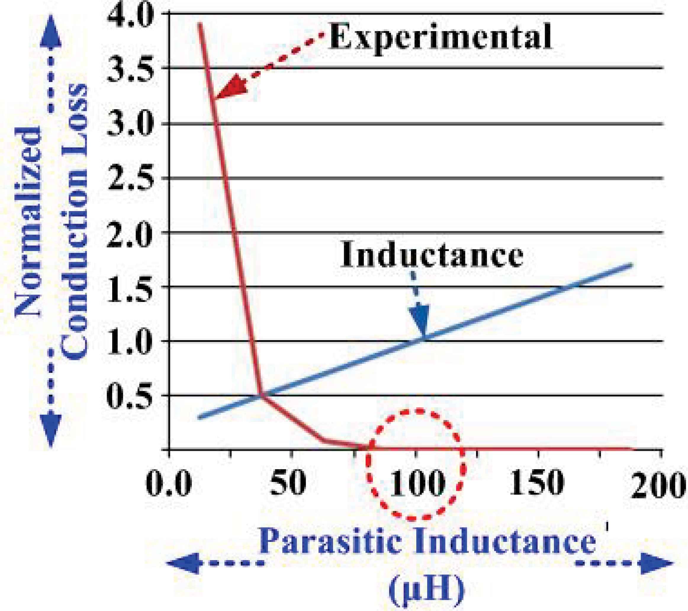
Plot showing conduction loss versus inductance variation.
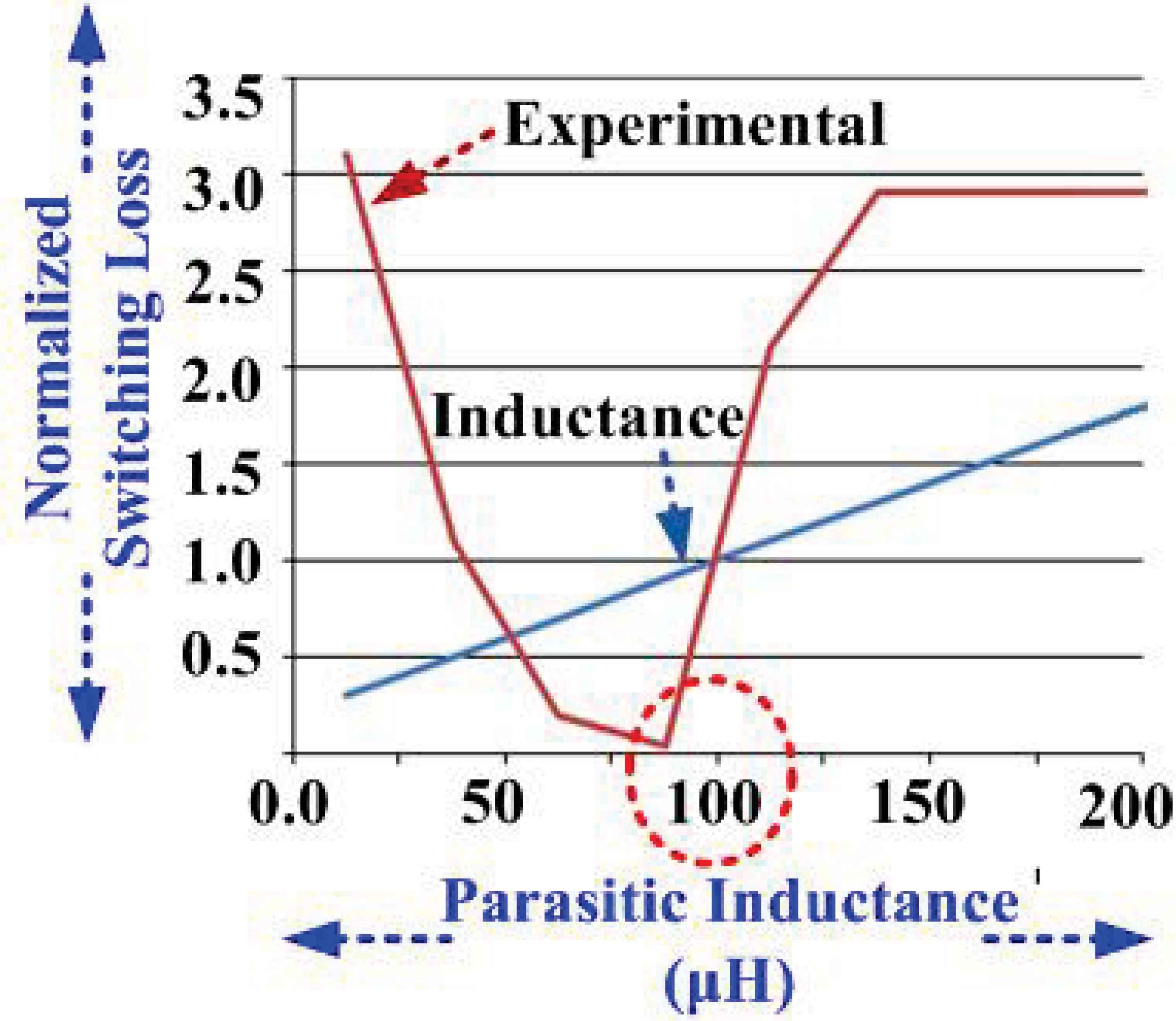
Plot showing switching loss versus inductance variation.
Finally, the performances obtained such as the higher output voltage and higher efficiency, reduced % ripple, which verifies that the proposed DC-DC converter (hardware prototype) has a better power density factor as per the standard [20–22]. This which in turn proves the exact viability for parasitic compensation and suits the high voltage industrial needs.
5. Control Strategies based on P-I and Fuzzy Logic
A standard closed-loop P-I controller scheme for the proposed EHV DC-DC boost converter is shown in Fig. 5. It notably consists of one stage voltage sensor feedback obtained from the dc load voltage. It is then compared with the set reference voltage VO,ref to obtain the error between reference DC bus voltage and feedback signal. Further, the error signal is applied to the P-I controller to compensate the available error. The manipulated signal thus obtained from the P-I controller defines the set duty ratio k and is compared with high frequency ramp-signal to generate the controlled pulse-width modulated (PWM) signal to the static switch S. The parameters (P-proportional gain, I-integral gain) are fine-tuned to get the set reference dc voltage under different perturbation conditions [11–12], [23–29].
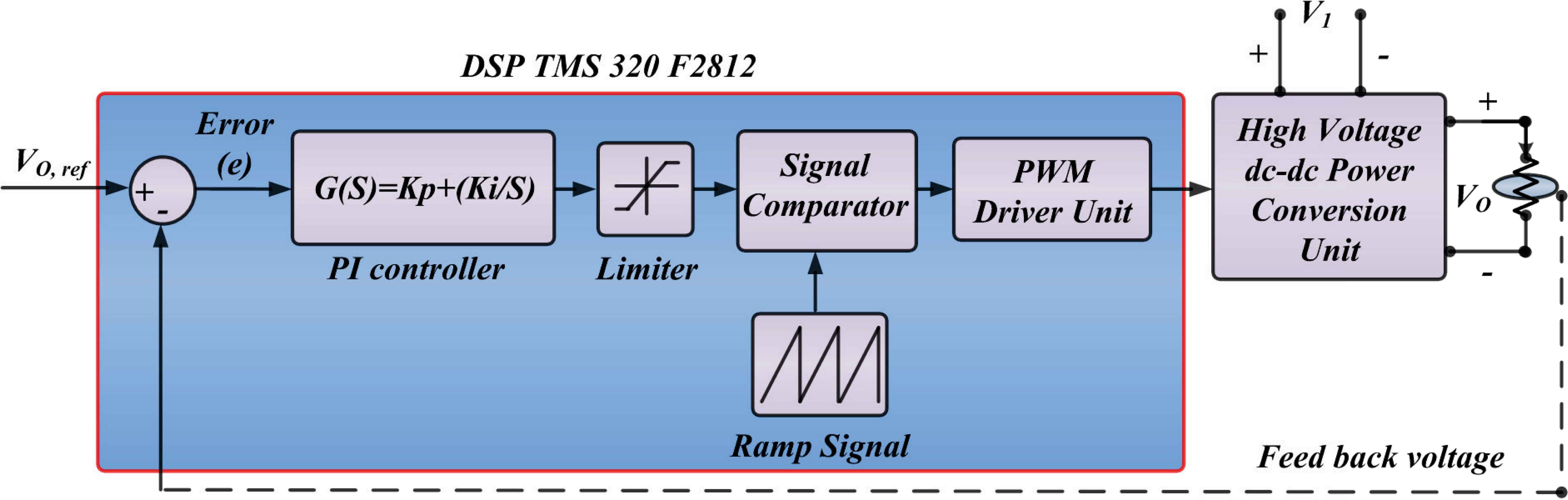
Simplified closed loop control strategy under line/load regulation using proportional-integral (P-I) control scheme.
The block diagram of generalized rule based fuzzy logic controller (FLC) is shown in Fig. 6(a), where e(k) and de(k) denote the input error and the rate of change in the input variables, respectively. The FLC block is composed of fuzzification interface, fuzzy rules, and inference and de-fuzzification mechanism. The FLC has two inputs which are error signal, e(k), and change in error signal, de(k). The output, c(k), on the other hand represents the control component to generate the switching signal for n-channel MOSFET switch.
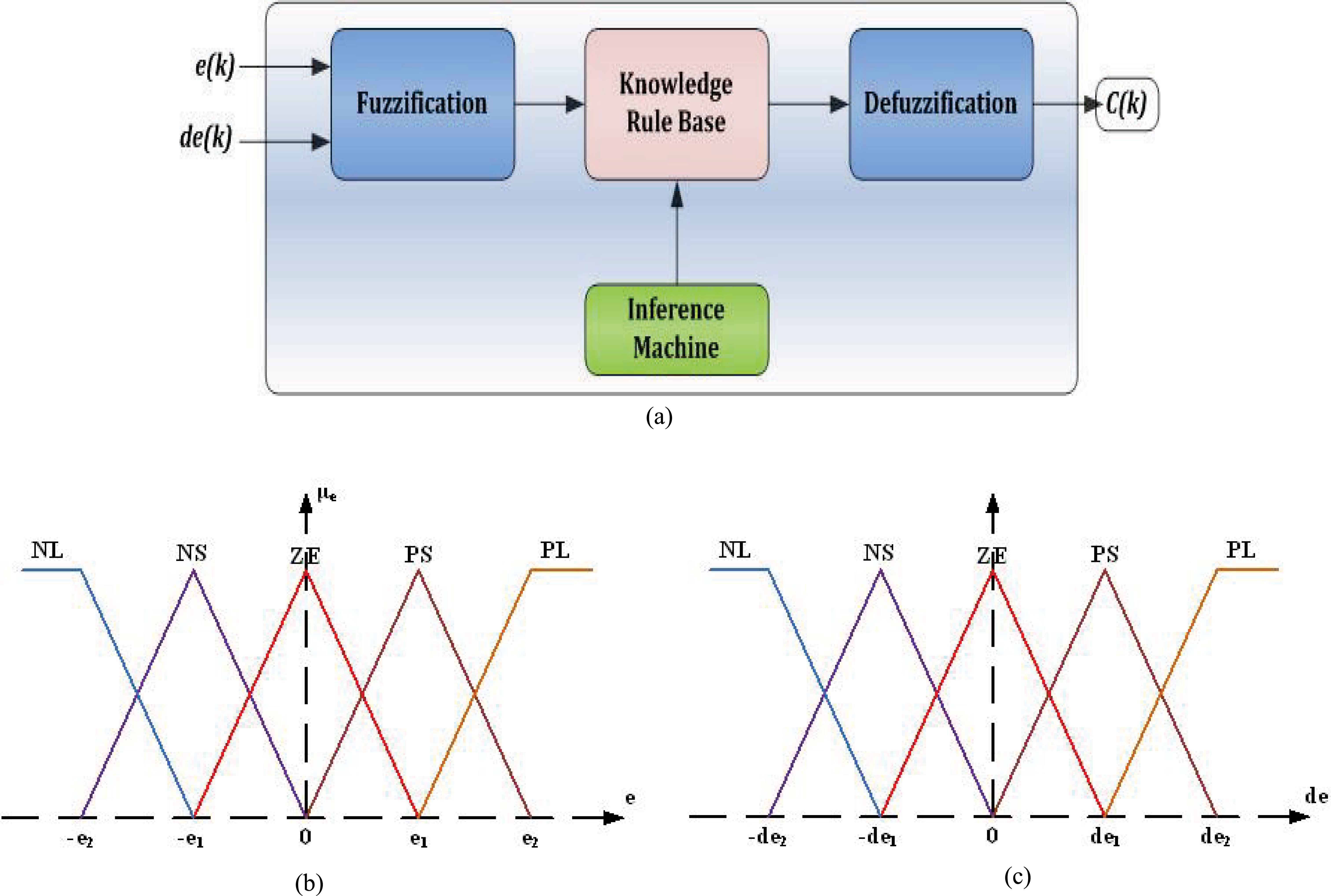
(a) Fuzzy logic rule based system generalized structure. Membership function of the fuzzy logic controller, (b) membership function of error (e), (c) membership function of change-in-error (de).
In the first stage, the crisp variables, e(k) and de(k), are converted into fuzzy variables such as E(k) and dE(k) using the triangular membership functions given by Fig. 6(b) and Fig. 6(c). Then, each universe of discourse is divided into five fuzzy sets: Namely, NL (negative large), NS (negative small), ZE (zero), PS (positive small) and PL (positive large). Each fuzzy variable is a member of the subsets with a degree of membership varying between 0 (non-member) and 1 (full-member) [30–32]. In the second stage of the FLC, the fuzzy variables, E(k) and dE(k), are processed by an inference engine that executes a set of control rules contained in a 5×5 rule bases as given by Table 4. These rules are designed based on the dynamic behavior of the error signal resulting in the symmetrical matrix. This is a general rule-based design with a 2-D phase plane. Each rule is expressed via the following form
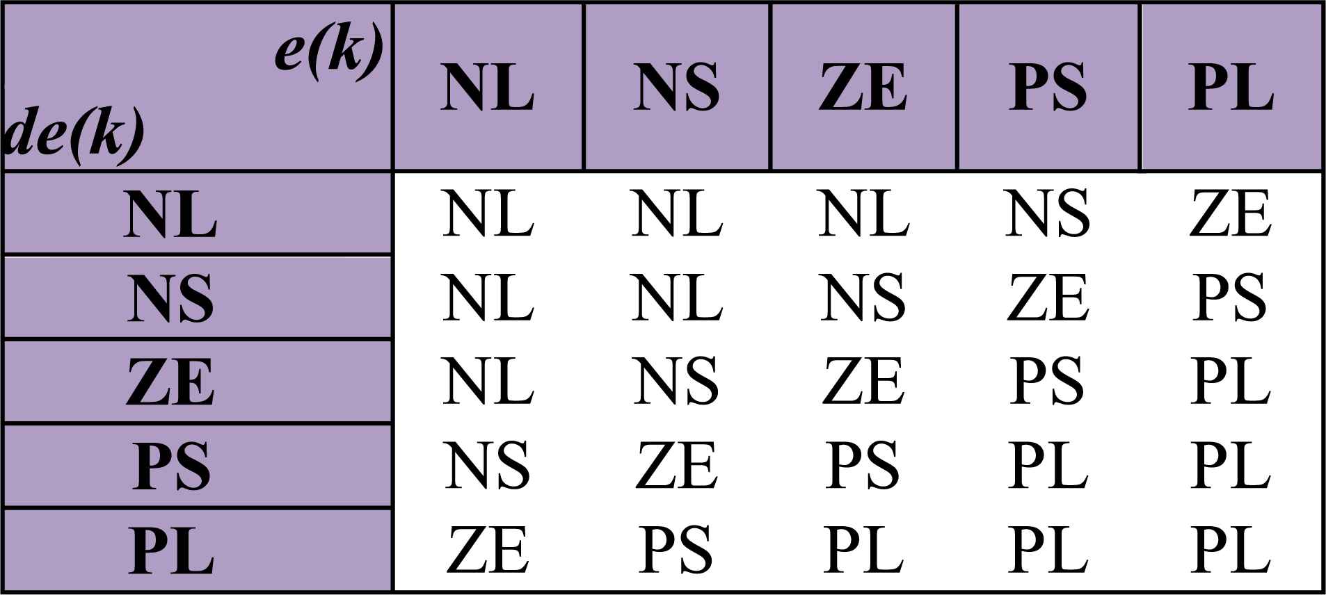
Matrix formulation (5x5) for fuzzy logic rules.
Different inference algorithms can be used to space the fuzzy set values for the output fuzzy variable, c(k). In this work, the max-min inference algorithm is used, in which the membership degree is equal to the maximum of the product of E and dE membership degree. The output variable from the inference engine is converted into a crisp value in the de-fuzzification stage. Various de-fuzzification algorithms have been proposed in the literature. In this work, the centroid de-fuzzification algorithm is used, in which the crisp value is calculated as the centre of gravity of the membership function. The definition of the spread of each partition, or conversely the width and symmetry of the membership functions, is generally a compromise between dynamic and steady state accuracy. Equally, spaced partitions and consequently symmetrical triangles are reasonable choices [30–32]. Complete control scheme based on fuzzy logic controller algorithm for the EHV DC-DC boost converter is illustrated by Fig. 7.
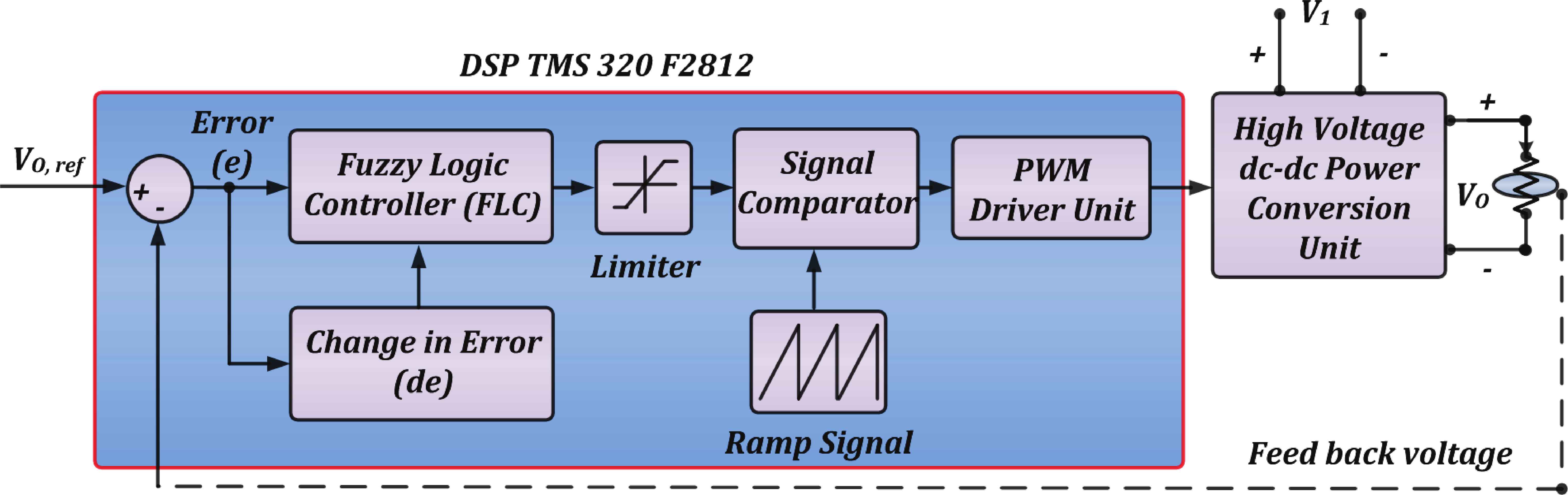
Simplified closed loop control strategy under line/load regulation using fuzzy logic control scheme.
6. Hardware Implementation and Experimental Results
Hardware prototype model of EHV DC-DC boost power converter is implemented as shown by Fig. 8 and based on parameter given by Table 2 with a digital signal processor (DSP) TMS320F2812 [26–28]. The control strategies based on P-I and fuzzy logic controller algorithm are framed in DSP that also generates the controlled PWM signal for N-channel MOSFET. The inductance and capacitance values of the power circuit are determined according to the criteria of 5% output ripple requirement as per IEEE standards [11–12], [27–29].
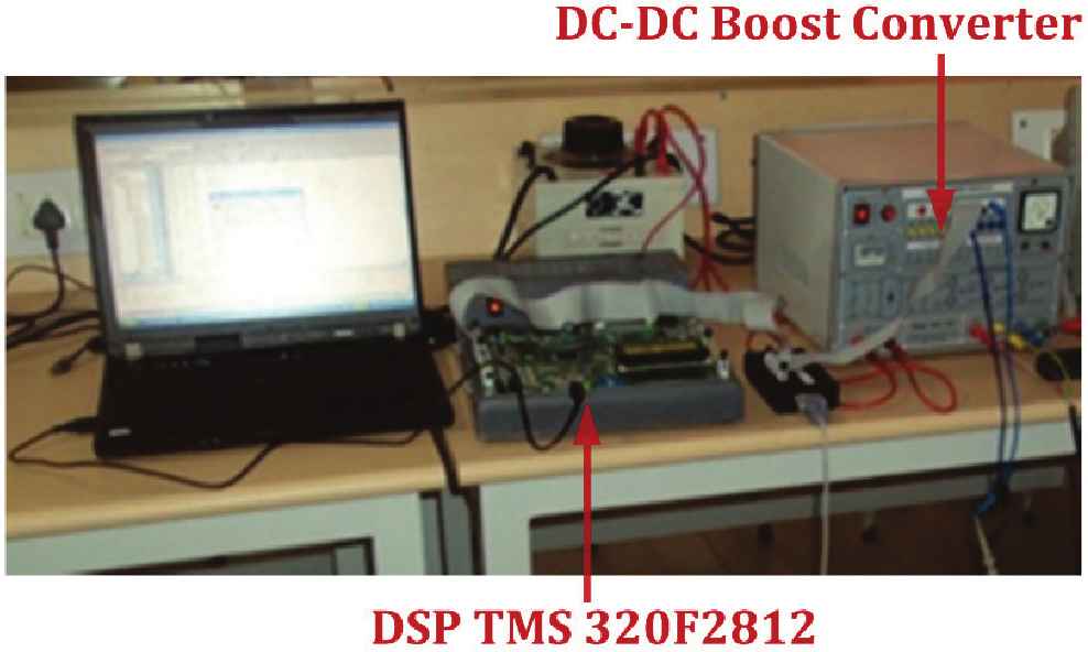
Hardware prototype module of EHV dc-dc boost power converter with DSP TMS320F2812 processor.
Fig. 9(a) and Fig. 9(b) shows the P-I controller based experimental results of output voltage and current at the rated conditions (set reference output voltage 120V, load resistance 44Ω and duty ratio k = 2/3). It is observed that the output voltage is slightly lower than the set reference and settles at 119.8V with 1.0833% peak overshoot, with 200mv steady state and 1 sec settling time, closely matches the prediction given by Eq. 12 at k = 2/3. Correspondingly, the output current is observed as 2.722A with 1.0833% peak overshoot and 1 sec settling time that closely matches the prediction given by Eq. 13.
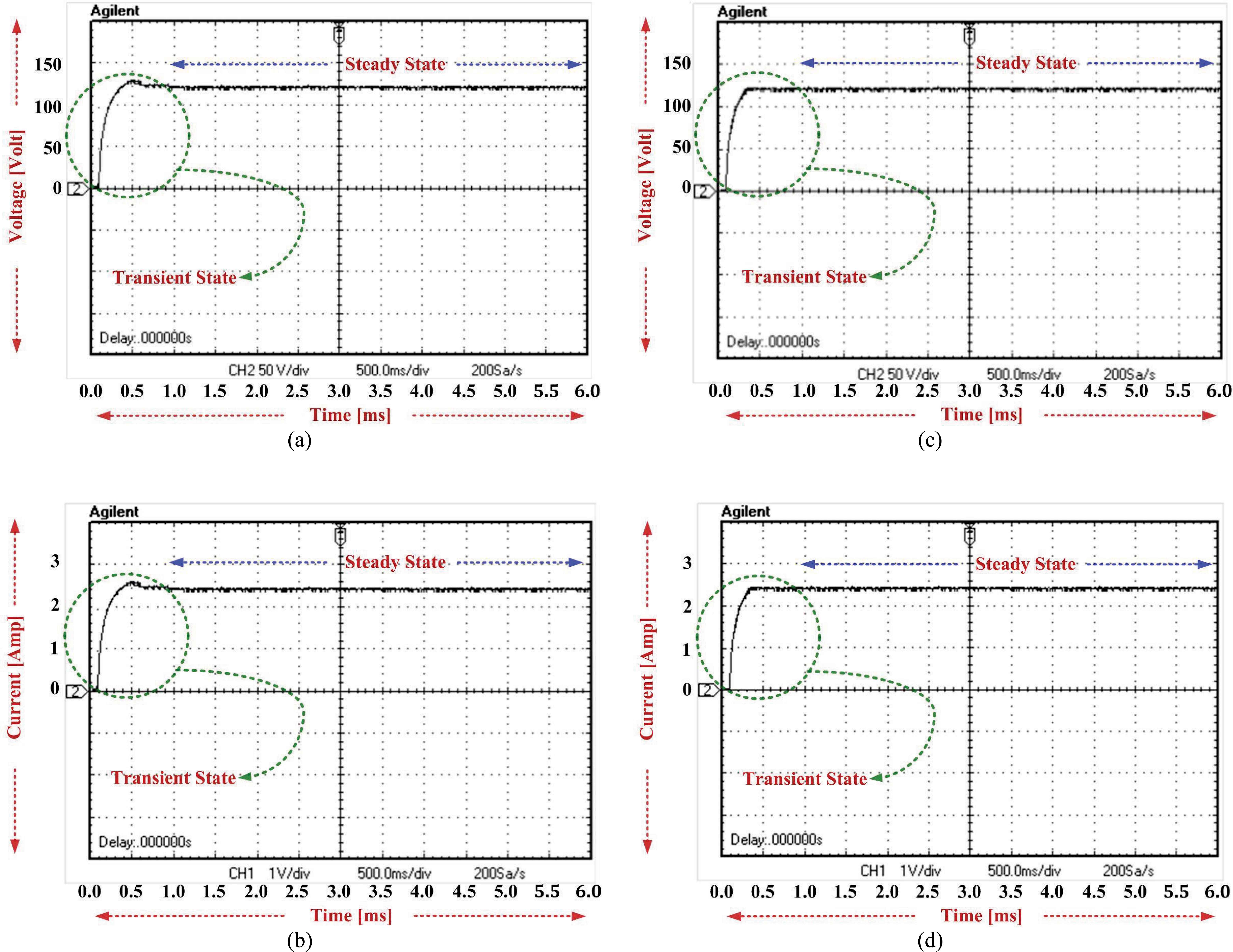
P-I and fuzzy controlled output performances of EHV power converter in transient and steady-state conditions. P-I: (a) output voltage, (b) output current. Fuzzy: (c) output voltage, (d) output current. [50v/div, 2A/div].
Fig. 9(c) and Fig. 9(d) show the fuzzy logic controller based experimental results of output voltage and current at the rated conditions. It is observed that the output voltage is slightly lower than the set reference that settles at 119.925V with 1.016% peak overshoot and 0.4 sec settling time, which closely meets the prediction given by Eq. 12 at k = 2/3. Correspondingly, the output current 2.7255A observed with 1.016% peak overshoot and 0.4 sec settling time, closely matches the prediction given by Eq. 13.
Fig. 10(a) and Fig. 10(b) show the P-I controller based experimental results of output voltage and current obtained under line and load perturbation condition. It is noticed that the output voltage and current are stabilized at 1 sec with a peak overshoot 1.125% when the battery voltage represents a step variation from 10V to 9V. Even though the load resistance varies from 48Ω to 44Ω, the output voltage retains the same value of 119.8V and current value of 2.722A which was observed with 1.125% peak overshoot and 1.2 sec settling time. The output voltage and current results closely match the prediction given by Eq. 12 and Eq. 13.
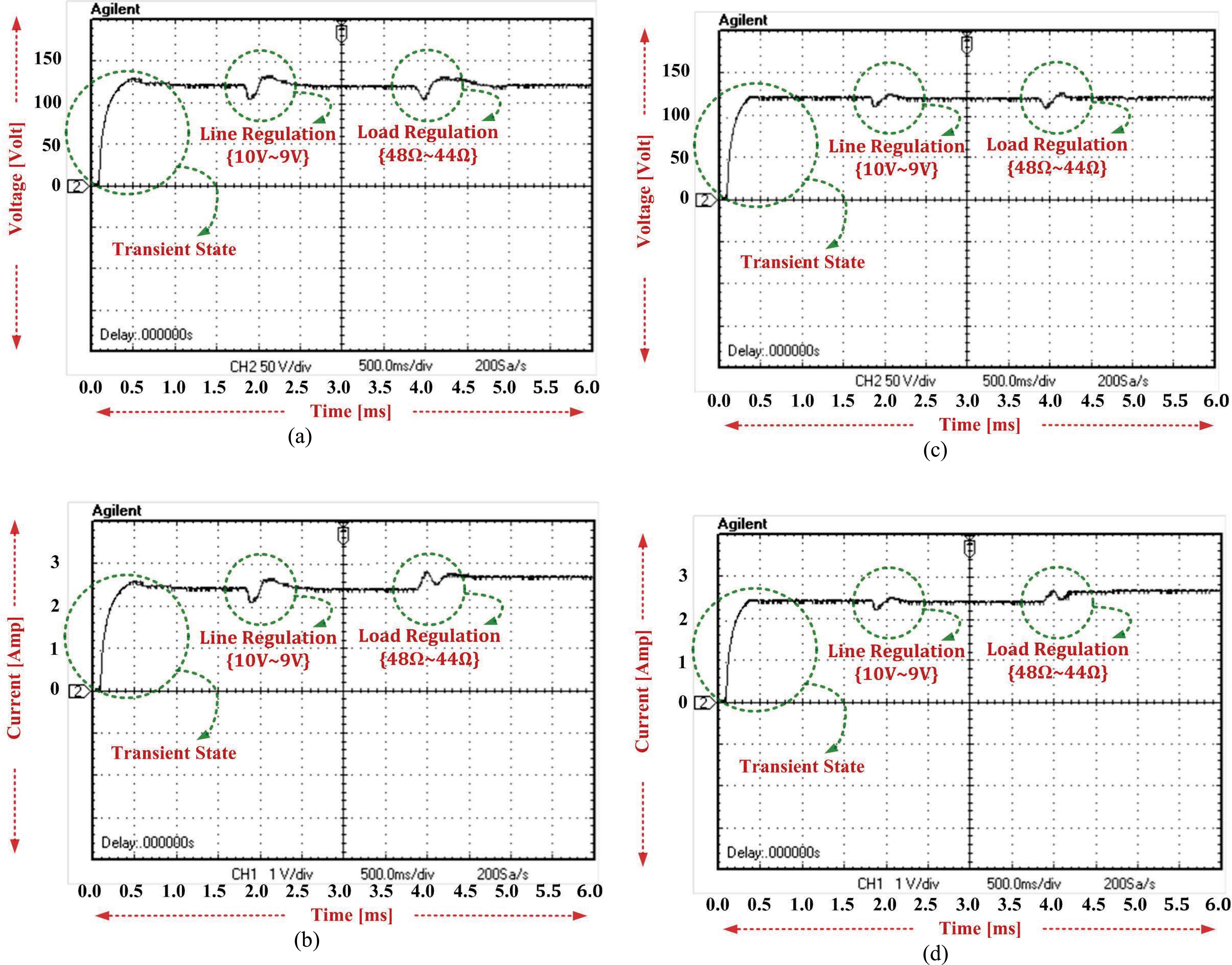
P-I and fuzzy controlled output performances of EHV power converter in transient, line/load regulation & steady-state conditions. P-I: (a) output voltage, (b) output current. Fuzzy: (c) output voltage, (d) output current. [50v/div, 2A/div].
Fig. 10(c) and Fig. 10(d) show the fuzzy logic controller based experimental results of output voltage and current obtained under line and load perturbation condition. It is noticed that the output voltage and current are stabilized at 0.28 sec with a peak overshoot 1.0416% when the battery voltage represents a step variation from 10V to 9V. Even though the load resistance varies from 48Ω to 44Ω, the output voltage retains the same value of 119.925V and current value of 2.7255A which was observed with 1.0666% peak overshoot and 0.25 sec settling time. The output voltage and current results closely match the prediction given by Eq. 12 and Eq. 13.
The experimental test results and information provided by Table 5 confirms that the control strategy based on fuzzy logic controller provides minimal peak overshoot with faster settling time and steady error accuracy in comparison to classical P-I controller. It is practically appreciable that the verified generated outputs of hardware prototype have losses in the range of milli-amplitude.
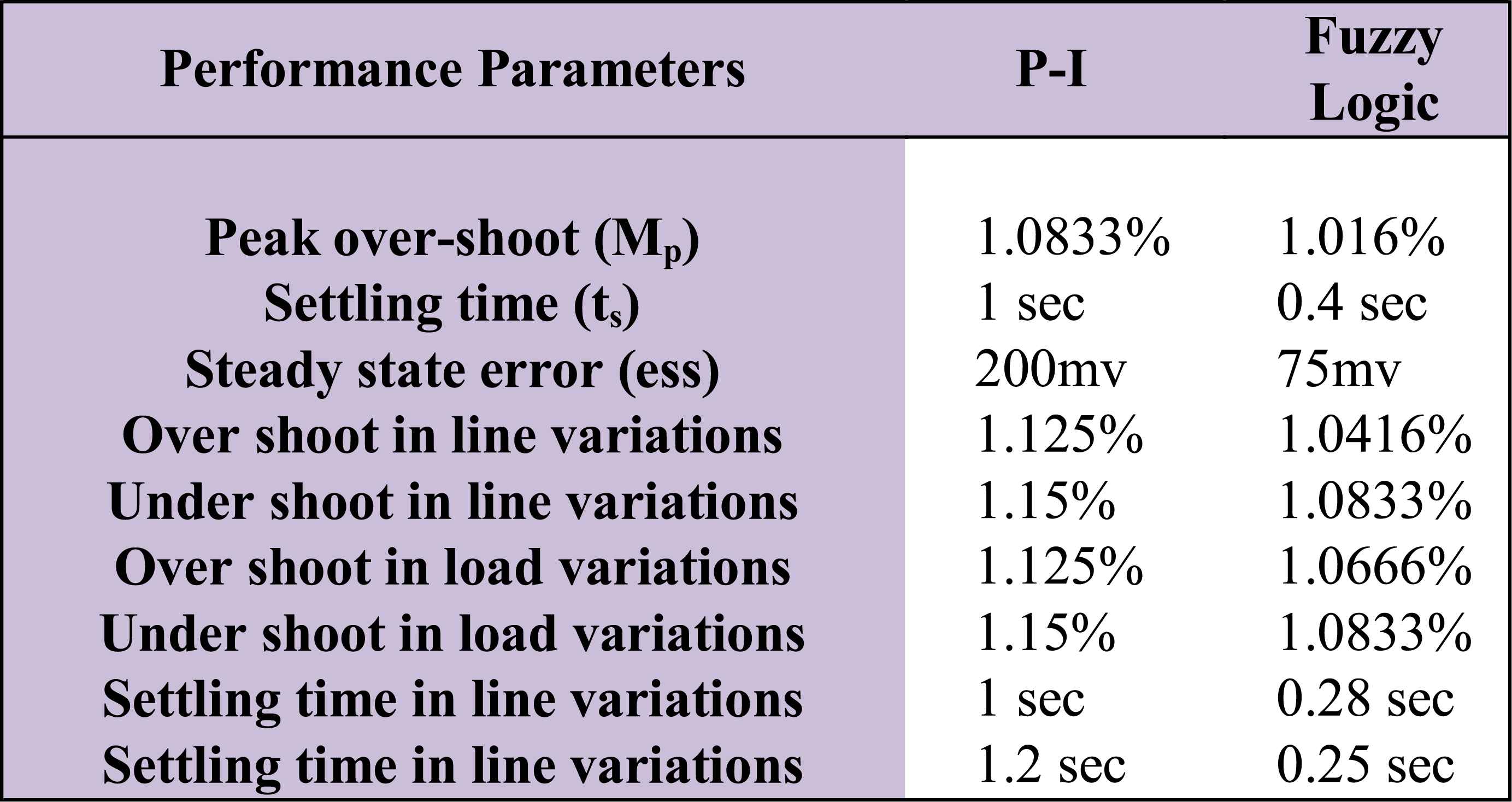
Performance comparison between P-I and fuzzy logic controller.
Finally, the higher output voltage and higher efficiency, reduced % ripple (Table 3) and faster settling time (Table 5), verify that the proposed dc-dc converter (hardware prototype) has better power density factor as per standard [20–23, 27–29]. Also notable that the output settles less than 1 sec in all investigation, yet still DSP has its own sampling rate to interface with external hardware modules in real time. This in turn proves the exact viability for parasitic compensation and suit the high voltage needs of HVDC transmission systems and high voltage industrial applications.
7. Conclusions
The comparative performance study of control strategies based on P-I and fuzzy logic closed-loop with single (voltage feed-back) sensor algorithm for EHV DC-DC boost power converter is presented in this paper. The extra high-voltage DC-DC power boost converter circuit has been integrated with voltage-lift technique to generate higher output voltage and significantly overcomes the deficiencies of parasitic effects with reduced ripples at the output waveforms (voltage/current).
Experimental results prove that the fuzzy logic controller provided good performances during transient, steady-state and line/load perturbation conditions in comparison to standard P-I controller. The investigated EHV DC-DC boost converter along with fuzzy logic based control strategy is suitable for HVDC transmission system where high-voltage becomes mandatory with reduced ripple at the output.
References
Cite this article
TY  - JOUR
AU  - Sanjeevikumar Padmanaban
AU  - Gabriele Grandi
AU  - Frede Blaabjerg
AU  - Pat Wheeler
AU  - Pierluigi Siano
AU  - Manel Hammami
PY  - 2017
DA  - 2017/01/01
TI  - A Comprehensive Analysis and Hardware Implementation of Control Strategies for High Output Voltage DC-DC Boost Power Converter
JO  - International Journal of Computational Intelligence Systems
SP  - 140
EP  - 152
VL  - 10
IS  - 1
SN  - 1875-6883
UR  - https://doi.org/10.2991/ijcis.2017.10.1.10
DO  - 10.2991/ijcis.2017.10.1.10
ID  - Padmanaban2017
ER  -