
Biomimetic Analog Silicon Synaptic Circuit with Tunable Reversal Potential
- DOI
- 10.2991/jrnal.k.200512.005How to use a DOI?
- Keywords
- Silicon neuronal networks; synaptic reversal potential; low-power
- Abstract
Experimental results of a biomimetic silicon synaptic circuit capable of generating both excitatory and inhibitory postsynaptic currents are presented. The generated synaptic current takes into account its first-order dependence on the instantaneous value of the postsynaptic membrane potential, with the synaptic current being proportional to the difference between a tunable synaptic reversal potential and the membrane potential of the postsynaptic neuron. None of the synaptic circuits proposed to date take this dependence into account over the range of biologically plausible synaptic reversal potentials and membrane potential. Special emphasis has been put on minimizing the static power consumption of the synaptic circuit, a design metric not yet analyzed or reported in most of the contemporary CMOS-based synaptic circuits.
- Copyright
- © 2020 The Authors. Published by Atlantis Press SARL.
- Open Access
- This is an open access article distributed under the CC BY-NC 4.0 license (http://creativecommons.org/licenses/by-nc/4.0/).
1. INTRODUCTION
Silicon Neuronal Networks (SNNs) [1–3] refers to a network of spiking neurons designed using silicon-based neuronal soma and synaptic circuits. Armed with local unsupervised learning rules such as Spike Timing Dependent Plasticity, they are a prime candidate to arrive at the goal of realizing autonomous learning machines addressing the major issues of high power consumption and von-Neumann bottleneck prevalent in contemporary computing architectures. These circuits are designed to mimic as closely as possible the electrophysiological dynamics of the neuronal cell body and synapses in the brain. Though various biologically realistic neuronal soma circuits have been proposed in the past, the need for a biomimetic synaptic circuit persists. The nervous system consists of a multitude of chemical synapses comprising various neurotransmitters (glutamate, GABA, etc.) which act on specific receptors on the postsynaptic membrane with low (GABAA, GABAB) or high (AMPA, NMDA) reversal potentials. Synapses are the key structures that localize memory as well as information processing in the nervous system, and biomimetic synaptic models have long been known to enhance the processing capability of the overall network to perform complex computational tasks [4]. In this manuscript, the experimental results of a low power biomimetic analog silicon synaptic circuit with pseudo-5-bit synaptic efficacy are presented. The circuits in the dawn approximated postsynaptic currents as pulses and neglected the exponential rising and decaying characteristics of these currents. Circuits proposed in the recent past have incorporated these temporal dynamics as well as focused on reducing the circuit footprint by having a single synapse circuit emulate multiple synapses. However, none of the low-power oriented circuits proposed to date take into account the experimentally observed first-order dependence of synaptic current on the difference between synaptic reversal potential and the instantaneous value of the membrane potential of the postsynaptic neuron. This phenomenological description of synaptic current is of paramount importance in implementing the experimentally observed phenomenon of shunting or silent inhibition. A few [3,5,6] synaptic circuits incorporate the effect of synaptic reversal potential but their implementation is not biomimetic as the current generated in these circuits is unidirectional. In addition to incorporating this effect, special emphasis has been put in the design to minimize the static power consumption of the synaptic circuit. As the synapses are activated in an event-based manner, a large scale SNN will have many synapses staying dormant at any particular time interval thus making static power consumption an important metric to be capitalized upon. The proposed circuit was designed in TSMC 250 nm process. The next section of this manuscript provides a brief description of the synaptic circuit along with the setup used for measurements, followed by results, discussion, and the planned future work.
2. SYNAPTIC MODEL
Kinetic models [7] of chemical synapses that describe the neurotransmitter kinetics are capable of precisely reproducing the experimentally observed dynamics of postsynaptic currents. Following the analysis in Destexhe et al. [7] and generalizing the response over various receptor types, a phenomenological description of the synaptic current is given by:
3. PROPOSED SYNAPTIC CIRCUIT
3.1. Operation and Description
The proposed synaptic circuit (Figure 1) can be compartmentalized into three major blocks, a binary-weighted Digital to Analog Converter (M1–M10), an integrator circuit similar to the log domain integrator [8] (Csyn and M11), and a transconductance stage (M12–M18) to simulate the first-order dependence of synaptic current described by Equation (1). All the transistors operate in the sub-threshold regime and the circuit functions as follows. The DAC activated by an input pulse at the node nVin, sources a current Iw into the node Vsyn charging it linearly. The strength of Iw depends on the synaptic weight controlled by the state of the binary bits (nWa–nW2) and the value of the bias voltage sVw. During the DAC activation Iw is given by (ignoring short channel effect):
The phenomenological model of Equation (1) to describe the synaptic current is thus realized. Here the first term (in bracket) represents the transconductance of the circuit, represented by gsyn in Equation (1). The source of the tail transistors is connected to the node Vref set to 20 mV. It minimizes the leakage current of the transconductance stage when the circuit is inactive (with Vsyn = 0 V).
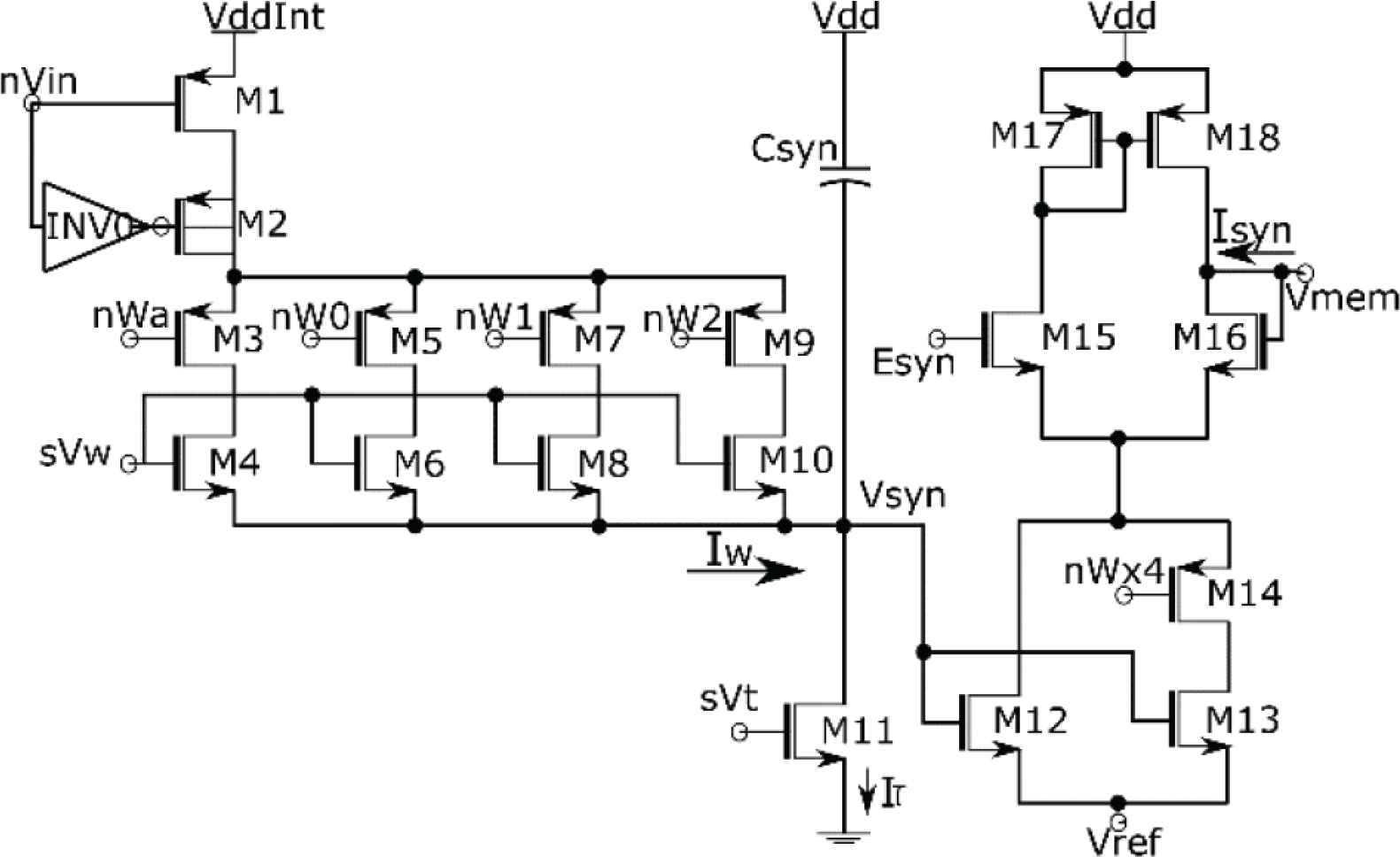
Schematic diagram of the proposed synaptic circuit. Dimensions of the transistors: M4 = 0.3758 * (w/l), M6 = w/l, M8 = 2 * (w/l) and M10 = 4 * (w/l) with w = 2 µm, l = 500 nm. Tail transistor M13 is three times wider than M12.
3.2. Design Methodology and Measurement Setup
To minimize the static power consumption the transconductance stage of the circuit was implemented using PMOS-based current mirrors (M17 and M18) which resulted in the use of NMOS transistors in the DAC and integrator stages, unlike the conventional log domain integrator circuit. Synapses due to their sheer large numbers occupy most of the silicon real estate in an SNN chip, thus it is most important to minimize the footprint of the synaptic circuit. The value of synaptic efficacy usually controlled by a DAC stage takes up the most area. Towards this endeavor, in contrast to the conventional design approach such as in Wang and Liu [9] and Moradi and Indiveri [10] where significant stress is put on the accuracy of DAC resolution leading to overhead in terms of area and static power consumption respectively, the DAC stage of the proposed circuit is relatively compact. This was achieved by trading off the accuracy of DAC resolution (see Figure 1 caption) using a combination of half- and full-sized transistors to construct it. As the bit resolution of biological synapses is still unknown, this approach was chosen making sure that its output changes monotonically with the change in the corresponding input synaptic efficacy, without significant stress on the accuracy of its resolution (i.e. the value of jump in the output per unit input change). The DAC stage arms the synaptic circuit with 4-bit of synaptic efficacy and the fifth bit is controlled by the node nWx4 in the transconductance stage. When turned on, the tail transistor M13 which is three times the size of M12 is activated thus resulting in a four times increase in the magnitude of the synaptic current. Table 1 lists down the synaptic weights given by the 5-bit input, nWa, nW0, nW1, nW2, and nWx4. We call it pseudo-5-bit as the total number of weight values we get is 27 instead of 32. In our circuit, instead of using 32 transistors to realize full 5-bit, we used seven full-sized transistors for M6, M8 and M10 and one half-size transistor for M4. This shrinks not only the footprint of these transistors but also that of M2 by reducing the charge injection phenomenon.
| nWx4 (MSB) | nW2 | nW1 | nW0 | nWa (LSB) | Weight value |
|---|---|---|---|---|---|
| 0 | 0 | 0 | 0 | 0 | 0 |
| 0 | 0 | 0 | 0 | 1 | 1 |
| . . . | . . . | . . . | . . . | . . . | . . . |
| 0 | 1 | 1 | 1 | 1 | 15 |
| 1 | 0 | 1 | 0 | 0 | 16 (4 × 4) |
| 1 | 0 | 1 | 0 | 1 | 20 (4 × 5) |
| 1 | 0 | 1 | 1 | 0 | 24 (4 × 6) |
| . . . | . . . | . . . | . . . | . . . | . . . |
| 1 | 1 | 1 | 1 | 1 | 60 (4 × 15) |
Pseudo 5-bit synaptic weights. Bit value of 0(1) corresponds to voltage of VddInt (0)
The fabricated chip consists of 128 synaptic circuits connected to a single qualitatively modeled [11] neuronal soma circuit. The scale of synaptic current in the proposed circuit was designed to interact with this silicon neuron circuit, whose membrane capacitance is about 900 fF. Since the membrane capacitance of the neuronal cells is about several hundreds of picofarads and the scale of synaptic currents is about several hundreds of picoamperes, the range of synaptic current of the proposed circuit is set to about 10 pA allowing a margin of about an order of magnitude. The synaptic circuits were laid out in groups of four each configured to mimic one of the four major neurotransmitters. Another group of 16 synapses, (hereafter referred to as TEG) were connected to a high resistance circuit designed using a transconductance amplifier with source degeneration to measure the synaptic current. A spike address decoder and register array were used to route spikes to designated synaptic inputs and store the synaptic weights respectively. These modules were configured using an onboard FPGA.
4. RESULTS
Unless specified otherwise, the results presented are from the synapses in the TEG and the voltage parameters listed in the caption of Figure 2 were used for measurement. The synaptic current was measured and plotted in terms of voltage across the high resistance circuit. Figure 3 shows the synaptic waveforms mimicking the response of the four major neurotransmitters. Figure 4 shows the plot of synaptic currents over the dynamic range of synaptic weights described in Table 1. The synapse was configured to be in excitatory mode with Esyn = 600 mV. Figure 2 demonstrates the first-order dependence of synaptic current on the difference between synaptic reversal potential (Esyn) and membrane potential (Vmem). Membrane potential was kept fixed at 700 mV (resting potential of neuronal soma). As expected from Equation (5) the relationship is approximately linear. Zero crossing occurs at around 707 mV instead of 700 mV due to the mismatch of transistors in the transconductance stage. The variation in the value of the time constant of the (falling phase of) synaptic waveform across the range of synaptic efficacy for different values of sVt is plotted in Figure 5. The maximum time constant obtained for the value of sVt = 0 V was on average around 175 ms with a standard deviation of 10.5% about the mean. The mean and the percentage standard deviation around the mean for the rest of the sVt values are labelled in Figure 5.
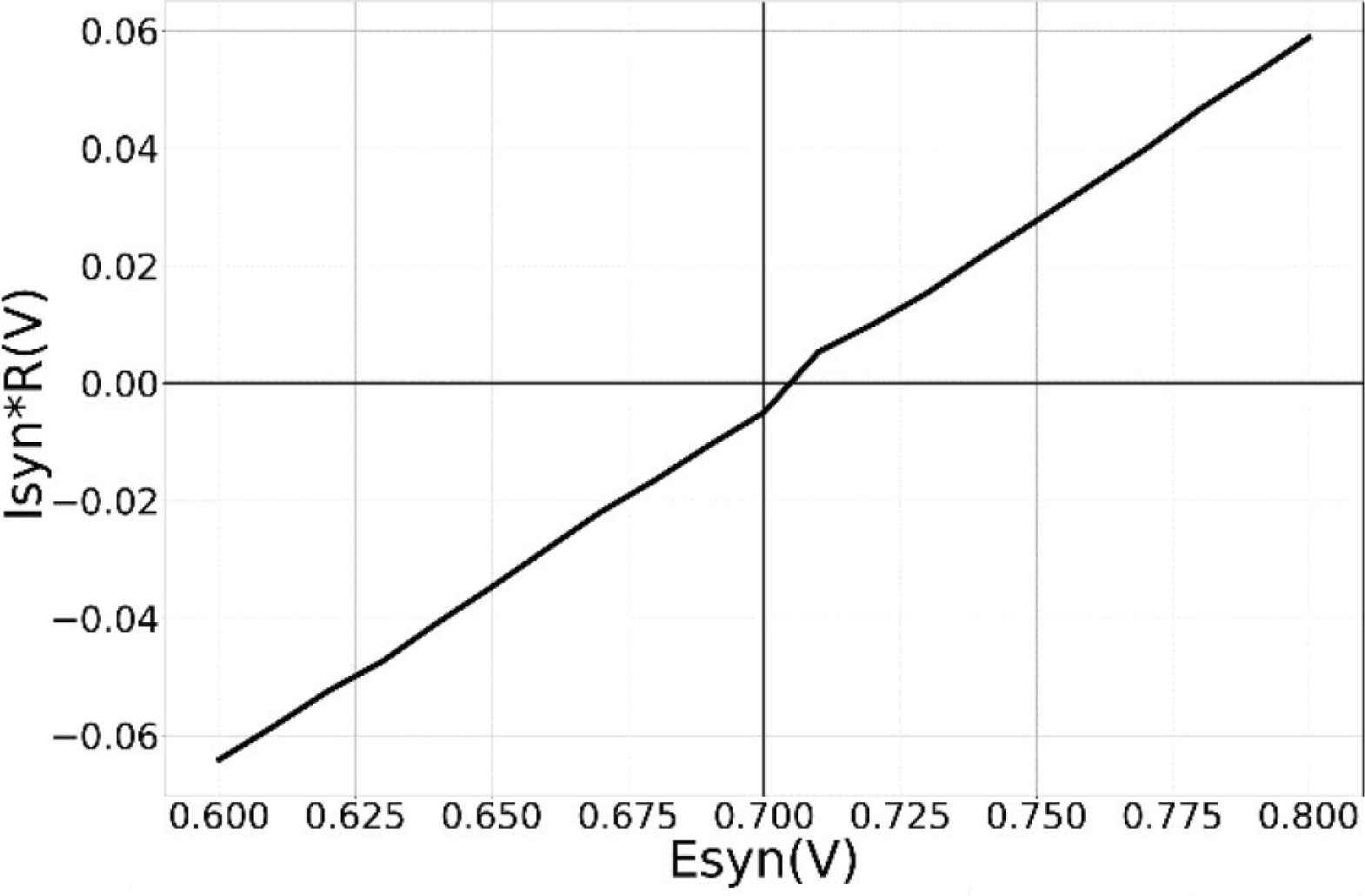
Dependence of synaptic current on synaptic reversal potential. Y-axis reflects the peak value of the synaptic current. Parameters used: sVw = 140 mV, sVt = 0, Esyn = 600 mV with maximum synaptic efficacy.
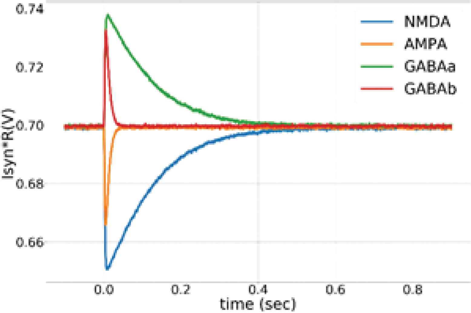
Synaptic currents emulating the response of excitatory neurotransmitters AMPA, NMDA (with Esyn = 600 mV) and inhibitory neurotransmitters GABAA, GABAB (with Esyn = 800 mV). sVt was set to 10 mV for NMDA and GABA mode and to 120 mV for AMPA and GABAA mode.
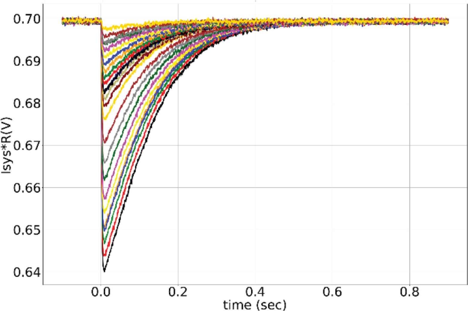
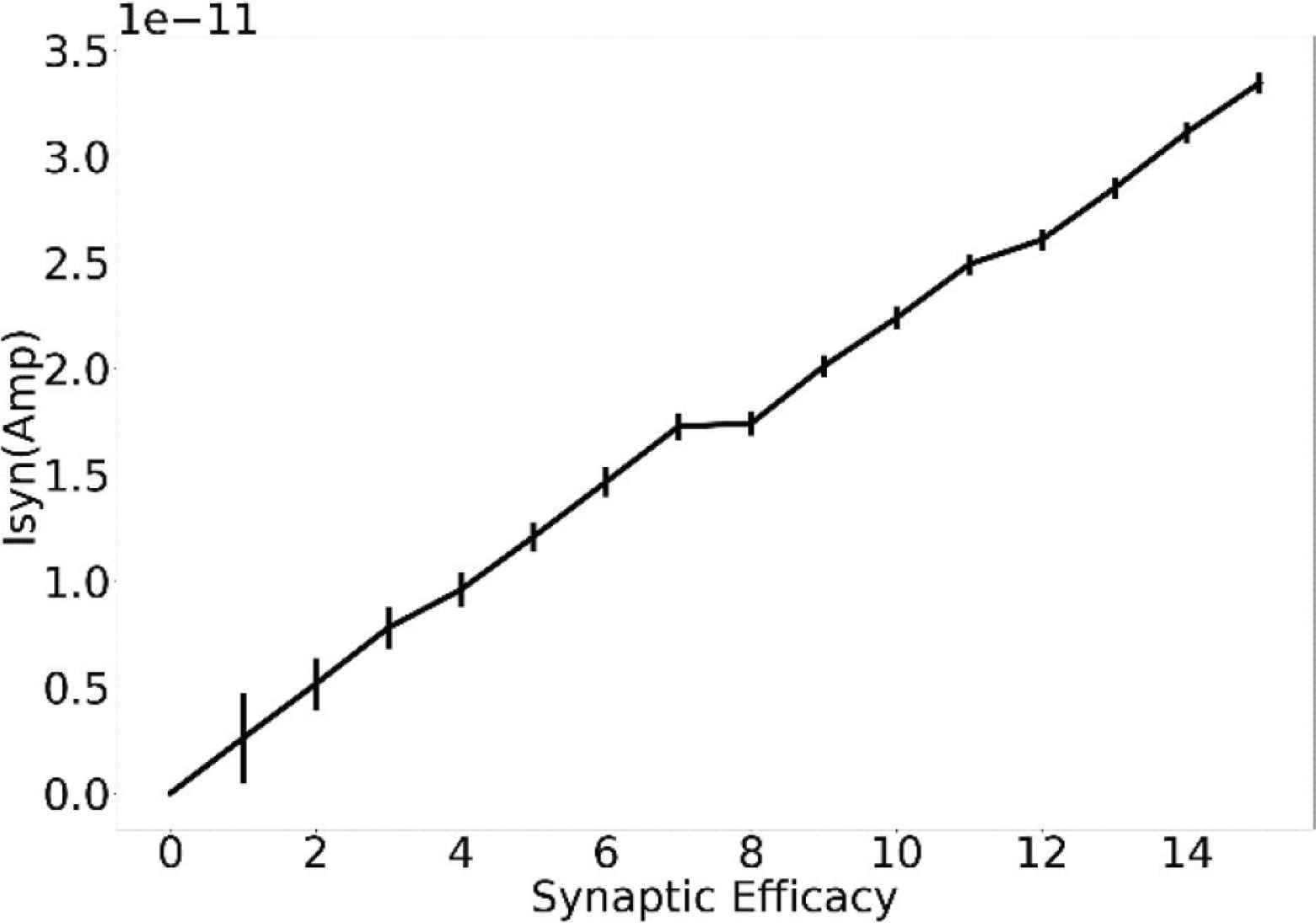
Synaptic current output over the dynamic range of the synaptic weights. Parameters used: sVw = 135 mV, sVt = 0, Esyn = 600 mV.
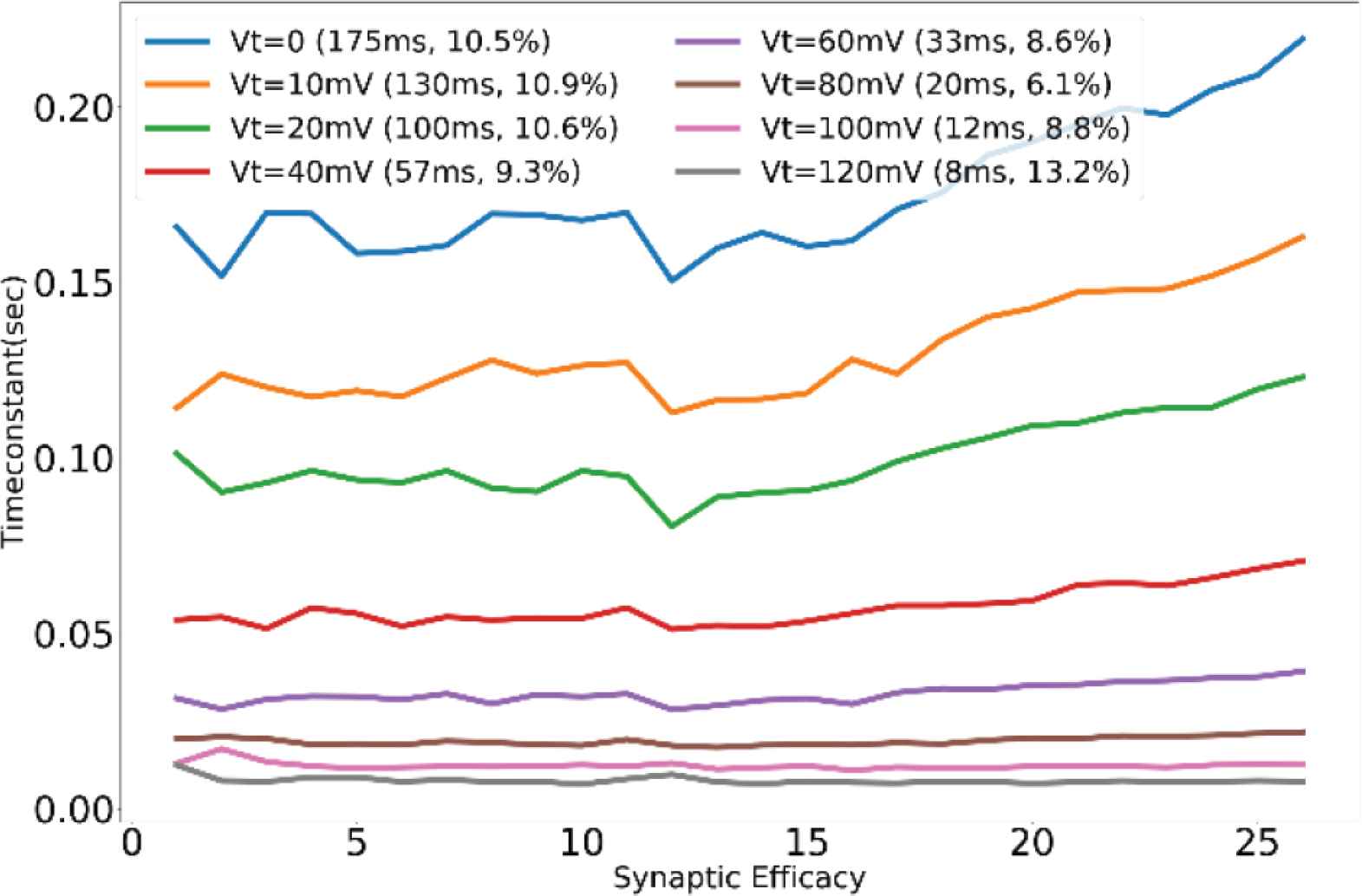
Profile of time constant for various values of sVt across the range of synaptic efficacy.
To characterize the mismatch and examine the desired monotonicity of the DAC stage, the following procedure was adopted. With the spiking circuitry of the neuronal soma deactivated, thus acting as a passive membrane, excitatory postsynaptic potential from 128 synaptic circuits was measured individually across the range of weight values of 4-bit binary-weighted DAC (from 0000 to 1111) giving a total of 2048 EPSPs. Due to the non-linear relationship between EPSP and EPSC an elaborate procedure involving current sources in the neuron circuit was used to construct a lookup table mapping the value of EPSP to corresponding EPSC. The mean and the standard deviation (represented by error bars) of the peak value of the synaptic current across the range of 4-bit synaptic efficacy for 128 synaptic circuits are plotted in Figure 6. Out of 128 synaptic circuits, a kink in the desired monotonicity was observed in 58 synapses between the synaptic efficacy value of 7(0111) and 8(1000). The maximum standard deviation was recorded to lie in between 5% and 20% of the mean value for maximum and minimum values of synaptic efficacy respectively (error bars at synaptic efficacy values 15 and 1 respectively).
Average value of the peak synaptic current for 128 synapses across the range of synaptic efficacy to characterize the DAC. Error bars capture variation across mean value of current.
The static power consumption of each circuit was limited to be under 2 pW and the dynamic energy consumption is measured as follows. For sVw = 110 mV (peak synaptic current of around 5 pA) and time constant of 160 ms, the input stage of our circuit consumes around 40 fJ per synaptic event and the integrator and the transconductance stage consume around 500 fJ (this value reduces to 112 fJ for a time constant of 3 ms).
5. DISCUSSION
As described above the deviation of EPSC intensity from the desired monotonicity with respect to the value of synaptic efficacy was observed between efficacy values of 7(0111) and 8(1000) for around 46% of the synaptic circuits. Around 6% of the synaptic circuits displayed deviation from monotonicity between the synaptic efficacy value of 3 and 4, and 11 and 12. The probable reason for this deviation is device mismatch combined with second-order and parasitic effects associated with the half-size transistor (M4 in Figure 1), but this could not be confirmed quantitatively due to the unavailability of statistical mismatch data in TSMC 250 nm CMOS PDK needed to perform Monte-Carlo simulation. The observed variation in standard deviation between the minimum and maximum values of synaptic efficacy is apparent from the size of transistors used in the DAC stage (see Figure 1 caption). For the synaptic efficacy value of 1, only the half-size transistor M4 (w = 750 nm, l = 500 nm) is active. As smaller devices exhibit higher mismatch, the standard deviation about the mean value of EPSC is higher in this case, and as the value of synaptic efficacy increases with additional full-size transistors M6 (w = 2 µm, l = 500 nm), M8 (w = 2 × 2 µm2, l = 500 nm) and M10 (w = 2 × 4 µm2, l = 500 nm) being activated the standard deviation about the mean decreases.
Data similar to one in Figure 6 but with the synaptic reversal potential value of set to 800 mV displayed higher standard deviation with respect to the mean value of the peak synaptic current. In other words the variance in the peak value of the synaptic current (measured for all synapses) for a particular value of synaptic efficacy was higher in the case of inhibitory synapses than in the case of excitatory ones. When configured in the inhibitory mode [(Esyn = 800 mV) > (Vmem = 700 mV)], most of the current sourced out of the Vmem node is activated through the path M15 → M17 → M18. The use of relatively short transistors (L = 400 nm) in the current mirror devices (M17 and M18) led to a higher mismatch among them throughout the synaptic array and thus higher standard deviation was observed. When configured in the excitatory mode [(Esyn = 600 mV) > (Vmem = 700 mV)], the current sourced into the node Vmem is activated through the shorter path consisting of M16. Due to their larger dimension, transistors M15 and M16 are better matched throughout the synaptic array and thus the standard deviation is smaller for synaptic circuits configured in the excitatory mode than in inhibitory mode. In other words, over the range of various reversal potential values, higher the contribution of current from transistor M18 into the node Vmem, which would depend on the relative difference between Esyn and Vmem, higher would be the standard deviation about the mean value of synaptic current throughout the synaptic array. As the transition frequency of the MOS transistor depends inversely on the square of its length, using a longer device leads to a sluggish synaptic response when configured in inhibitory mode (due to the relatively long path taken by the current). Making a trade-off between the response time and the probable mismatch effects, the length of the transistors was chosen to be 400 nm. This mismatch along with the Drain Induced Barrier Leakage effect on M18 led to a higher leakage current in the case synapses configured in inhibitory mode than in excitatory mode, also resulting in the offset in the zero-crossing observed in Figure 4. Though this additional leakage current can be compensated in the soma circuit, this difference needs to be minimized. One possible way which was verified via simulation was to separately control the bulk voltage of the current mirror transistors and fix it at a value higher than Vdd.
A standard deviation of about 10% around the mean value was observed in the time constants over the range of synaptic efficacy for various sVt values (Figure 5). This variation arises due to the transition of the operating region of the transistor M11 from saturation to linear during the discharging phase of the node Vsyn. Ideally during the discharge phase, the transistor M11 should be sinking a constant current depending only on the value of applied bias voltage sVt independent of its drain voltage (Vsyn), but the transistor deviates from this ideal behavior for smaller values of Vsyn and the current drawn decreases. The node Vsyn charges up to different voltage levels for different values of synaptic efficacy, thus during the discharge phase there is a variation in the value of time constant across the range of synaptic efficacy, even if the value of the bias voltage sVt is kept constant.
6. CONCLUDING REMARKS
Experimental results of a low power biomimetic silicon synaptic circuit fabricated in TSMC 250 nm technology node was presented. The circuit is the first low power synaptic circuit that takes into account the effect of synaptic reversal potential and the instantaneous membrane potential of the postsynaptic neuron on the synaptic current. To capitalize on the event-based nature of neuronal communication the design focused on minimizing static power consumption of the synaptic circuit, a metric not yet evaluated or reported in almost all contemporary CMOS based synaptic circuits. This first-generation chip contains only 128 synapses with just one input stage per integrator. The number of input stages can be increased to a higher number, the design is completely modular. Thus the number of synapses can be expanded by placing additional silicon synaptic modules. Issues related to device mismatch in the DAC and the transconductance stage were characterized and will be fixed in the future.
CONFLICTS OF INTEREST
The authors declare they have no conflicts of interest.
ACKNOWLEDGMENTS
This study was supported by NEC Corporation and DLab, The University of Tokyo in collaboration with Cadence Design Systems, Inc.
AUTHORS INTRODUCTION
Mr. Ashish Gautam
 He received his Bachelor of Technology degree in Electronics & Instrumentation Engineering in 2012 from Pondicherry University, Puducherry, India. He has worked as a Mixed Signal Design Engineer in the semiconductor industry for a period of approximately four years until 2016. He received his Master of Engineering degree in 2018 from the University of Tokyo, Japan where he is currently a second-year PhD student.
Dr. Takashi Kohno
 He has been with the Institute of Industrial Science at the University of Tokyo, Japan since 2006, where he is currently a Professor. He received the BE degree in Medicine in 1996 and the PhD degree in Mathematical Engineering in 2002 from the University of Tokyo, Japan.
REFERENCES
Cite this article
TY  - JOUR
AU  - Ashish Gautam
AU  - Takashi Kohno
PY  - 2020
DA  - 2020/05/15
TI  - Biomimetic Analog Silicon Synaptic Circuit with Tunable Reversal Potential
JO  - Journal of Robotics, Networking and Artificial Life
SP  - 22
EP  - 26
VL  - 7
IS  - 1
SN  - 2352-6386
UR  - https://doi.org/10.2991/jrnal.k.200512.005
DO  - 10.2991/jrnal.k.200512.005
ID  - Gautam2020
ER  -